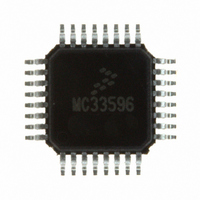
MC33596FJE Freescale Semiconductor, MC33596FJE Datasheet - Page 26

MC33596FJE
Manufacturer Part Number
MC33596FJE
Description
IC RECEIVER UHF PLL TUNED 32LQFP
Manufacturer
Freescale Semiconductor
Type
Receiverr
Datasheet
1.MC33596FCAE.pdf
(70 pages)
Specifications of MC33596FJE
Frequency
304, 315, 426, 434, 868 & 915MHz
Sensitivity
-104dBm
Data Rate - Maximum
22.4 kBaud
Modulation Or Protocol
FSK, OOK
Applications
General Data Transfer
Current - Receiving
10.3mA
Data Interface
PCB, Surface Mount
Antenna Connector
PCB, Surface Mount
Voltage - Supply
2.7 V ~ 3.6 V, 4.5 V ~ 5.5 V
Operating Temperature
-40°C ~ 85°C
Package / Case
32-LQFP
Operating Frequency
915 MHz
Operating Supply Voltage
3.3 V or 5 V
Maximum Operating Temperature
+ 85 C
Minimum Operating Temperature
- 40 C
Mounting Style
SMD/SMT
Operating Temperature (min)
-40C
Operating Temperature (max)
85C
Operating Temperature Classification
Industrial
Modulation Type
FSK/OOK
Package Type
LQFP
Operating Supply Voltage (min)
2.7V
Lead Free Status / RoHS Status
Lead free / RoHS Compliant
Features
-
Memory Size
-
Lead Free Status / Rohs Status
Lead free / RoHS Compliant
Available stocks
Company
Part Number
Manufacturer
Quantity
Price
Part Number:
MC33596FJE
Manufacturer:
FREESCALE
Quantity:
20 000
Part Number:
MC33596FJER2
Manufacturer:
FREESCALE
Quantity:
20 000
Configuration Mode
13
13.1 Description
This mode is used to write or read the internal registers of the MC33596.
As long as a low level is applied to CONFB and a high level to STROBE (see
master node driving the SCLK input, the MOSI line input, and the MISO line output. Whatever the
direction, SPI transfers are 8-bit based and always begin with a command byte, which is supplied by the
MCU on MOSI. To be considered as a command byte, this byte must come after a falling edge on CONFB.
Figure 18
Bits N[1:0] specify the number of accessed registers, as defined in
Bits A[4:0] specify the address of the first register to access. This address is then incremented internally
by N after each data byte transfer.
R/W specifies the type of operation:
Thus, this bit is associated with the presence of information on MOSI (when writing) or MISO (when
reading).
Figure 19
a slave. A received byte is considered internally on the eighth falling edge of SCLK. Consequently, the last
received bits, which do not form a complete byte, are lost.
Refer to
If several SPI accesses are done, a high and low level is applied to CONFB, and so on. By applying a high
level to STROBE, the MC33596 never enters standby mode. If there is no way to configure the level on
STROBE, the time interval between two SPI accesses must be less than one digital clock period T
26
Bit Name
0 = Read
1 = Write
Section 19.8, “Digital Interface
Configuration Mode
and
shows the content of the command byte.
Figure 20
Bit 7
N1
show write and read operations in a typical SPI transfer. In both cases, the SPI is
Bit 6
N0
N[1:0]
Table 7. Number N of Accessed Registers
00
01
10
11
Figure 18. Command Byte
Bit 5
MC33596 Data Sheet, Rev. 4
Timing,” to view the timing definition for SPI communication.
A4
Number N of Accessed Registers
Bit 4
A3
1
2
4
8
Bit 3
A2
Table
Bit 2
A1
7.
Figure
Bit 1
A0
Freescale Semiconductor
2), the MCU is the
Bit 0
R/W
digclk
.


