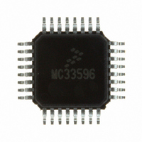
MC33596FJE Freescale Semiconductor, MC33596FJE Datasheet - Page 34

MC33596FJE
Manufacturer Part Number
MC33596FJE
Description
IC RECEIVER UHF PLL TUNED 32LQFP
Manufacturer
Freescale Semiconductor
Type
Receiverr
Datasheet
1.MC33596FCAE.pdf
(70 pages)
Specifications of MC33596FJE
Frequency
304, 315, 426, 434, 868 & 915MHz
Sensitivity
-104dBm
Data Rate - Maximum
22.4 kBaud
Modulation Or Protocol
FSK, OOK
Applications
General Data Transfer
Current - Receiving
10.3mA
Data Interface
PCB, Surface Mount
Antenna Connector
PCB, Surface Mount
Voltage - Supply
2.7 V ~ 3.6 V, 4.5 V ~ 5.5 V
Operating Temperature
-40°C ~ 85°C
Package / Case
32-LQFP
Operating Frequency
915 MHz
Operating Supply Voltage
3.3 V or 5 V
Maximum Operating Temperature
+ 85 C
Minimum Operating Temperature
- 40 C
Mounting Style
SMD/SMT
Operating Temperature (min)
-40C
Operating Temperature (max)
85C
Operating Temperature Classification
Industrial
Modulation Type
FSK/OOK
Package Type
LQFP
Operating Supply Voltage (min)
2.7V
Lead Free Status / RoHS Status
Lead free / RoHS Compliant
Features
-
Memory Size
-
Lead Free Status / Rohs Status
Lead free / RoHS Compliant
Available stocks
Company
Part Number
Manufacturer
Quantity
Price
Part Number:
MC33596FJE
Manufacturer:
FREESCALE
Quantity:
20 000
Part Number:
MC33596FJER2
Manufacturer:
FREESCALE
Quantity:
20 000
Register Description
The change of duration of one state (due to the STROBE pin level or a message being received) has no
influence on the timing of the following states (A, B, or OFF).
16
This section discusses the internal registers, which are composed of two classes of bits.
All registers can be accessed by the SPI. These registers are described below.
At power-on, the POR resets all registers to a known value (in the shaded rows in the following tables).
This defines the MC33596’s default configuration.
16.1 Configuration Registers (Description Bank A only)
Figure 24
RESET is a global reset. The bit is cleared internally, after use.
SL (Switch Level) selects the active level of the SWITCH output pin.
34
Reset Value
Bit Name
•
•
•
•
Access
If strobe pin is 0 the state is OFF.
If strobe pin is released from 0 while state is OFF, the initial OFF period is completed.
Configuration and command bits allow the MC33596 to operate in a suitable configuration.
Status bits report the current state of the system.
0 = no action
1 = reset all registers and counters
Register Description
describes configuration register 1, CONFIG1.
LOF1
Bit 7
R/W
1
Carrier Frequency
Table 8. LOF[1:0] and CF[1:0] Setting Versus Carrier Frequency
304 MHz
315 MHz
426 MHz
434 MHz
868 MHz
915 MHz
LOF0
Bit 6
R/W
0
Bit 5
CF1
R/W
Figure 24. CONFIG1 Register
0
MC33596 Data Sheet, Rev. 4
LOF1
0
1
0
0
0
1
Bit 4
CF0
R/W
1
RESET
LOF0
Bit 3
R/W
0
0
1
1
1
1
0
Bit 2
R/W
CF1
SL
0
0
0
0
0
1
1
LVDE
Bit 1
R/W
0
CF0
0
0
1
1
1
1
Freescale Semiconductor
CLKE
Bit 0
R/W
1
Addr
$00


