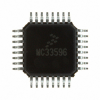
MC33596FJE Freescale Semiconductor, MC33596FJE Datasheet - Page 32

MC33596FJE
Manufacturer Part Number
MC33596FJE
Description
IC RECEIVER UHF PLL TUNED 32LQFP
Manufacturer
Freescale Semiconductor
Type
Receiverr
Datasheet
1.MC33596FCAE.pdf
(70 pages)
Specifications of MC33596FJE
Frequency
304, 315, 426, 434, 868 & 915MHz
Sensitivity
-104dBm
Data Rate - Maximum
22.4 kBaud
Modulation Or Protocol
FSK, OOK
Applications
General Data Transfer
Current - Receiving
10.3mA
Data Interface
PCB, Surface Mount
Antenna Connector
PCB, Surface Mount
Voltage - Supply
2.7 V ~ 3.6 V, 4.5 V ~ 5.5 V
Operating Temperature
-40°C ~ 85°C
Package / Case
32-LQFP
Operating Frequency
915 MHz
Operating Supply Voltage
3.3 V or 5 V
Maximum Operating Temperature
+ 85 C
Minimum Operating Temperature
- 40 C
Mounting Style
SMD/SMT
Operating Temperature (min)
-40C
Operating Temperature (max)
85C
Operating Temperature Classification
Industrial
Modulation Type
FSK/OOK
Package Type
LQFP
Operating Supply Voltage (min)
2.7V
Lead Free Status / RoHS Status
Lead free / RoHS Compliant
Features
-
Memory Size
-
Lead Free Status / Rohs Status
Lead free / RoHS Compliant
Available stocks
Company
Part Number
Manufacturer
Quantity
Price
Part Number:
MC33596FJE
Manufacturer:
FREESCALE
Quantity:
20 000
Part Number:
MC33596FJER2
Manufacturer:
FREESCALE
Quantity:
20 000
Configuration Switching
15.1.2.2 BANKA = 0, BANKB = 1
If strobe pin is 1, configuration is defined by Bank B, BANKS = 0.
If strobe pin is 0, MC33596 configuration is OFF.
If a message is received during State B, current state remains State B up to end of message.
15.1.2.3 BANKA = 1, BANK B = 1
If strobe pin is 1, configuration is defined by BANKS. BANKS is toggled at each falling edge of the strobe
pin.
If strobe pin is 0, MC33596 configuration is OFF.
If a message is received during state A or state B, current state remains the same up to end of message.
If a read or write access is done using SPI, the next sequence will begin with state A whatever was the
active state before SPI access by MCU.
15.1.3 Strobe Oscillator Switch Control
The conditions to enter strobe oscillator switch control are:
By simply writing BANKA and BANKB, the active banks will be defined.
The MCU can override strobe oscillator control by controlling the strobe pin level. If MCU I/O port is in
high impedance, the strobe oscillator will control the OFF/ON state of the MC33596. The various
available sequences are described in the following subsections.
32
Strobe Pin
Banks Bit
Strobe Pin
State A
•
•
•
State B
BANKA
Strobe pin connected to an external capacitor to define timing (see
On/Off
Strobe pin can also be connected to the MCU I/O port
SOE bit = 1
X
0
1
BANKB
OFF
Control”)
0
1
1
OFF
Bank A is active
Bank B is active
Bank A and Bank B are both active, configuration will toggle at each wakeup
State B
MC33596 Data Sheet, Rev. 4
State B
OFF
Section 11.3, “Receiver
OFF
State A
Freescale Semiconductor


