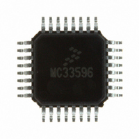
MC33596FJE Freescale Semiconductor, MC33596FJE Datasheet - Page 62

MC33596FJE
Manufacturer Part Number
MC33596FJE
Description
IC RECEIVER UHF PLL TUNED 32LQFP
Manufacturer
Freescale Semiconductor
Type
Receiverr
Datasheet
1.MC33596FCAE.pdf
(70 pages)
Specifications of MC33596FJE
Frequency
304, 315, 426, 434, 868 & 915MHz
Sensitivity
-104dBm
Data Rate - Maximum
22.4 kBaud
Modulation Or Protocol
FSK, OOK
Applications
General Data Transfer
Current - Receiving
10.3mA
Data Interface
PCB, Surface Mount
Antenna Connector
PCB, Surface Mount
Voltage - Supply
2.7 V ~ 3.6 V, 4.5 V ~ 5.5 V
Operating Temperature
-40°C ~ 85°C
Package / Case
32-LQFP
Operating Frequency
915 MHz
Operating Supply Voltage
3.3 V or 5 V
Maximum Operating Temperature
+ 85 C
Minimum Operating Temperature
- 40 C
Mounting Style
SMD/SMT
Operating Temperature (min)
-40C
Operating Temperature (max)
85C
Operating Temperature Classification
Industrial
Modulation Type
FSK/OOK
Package Type
LQFP
Operating Supply Voltage (min)
2.7V
Lead Free Status / RoHS Status
Lead free / RoHS Compliant
Features
-
Memory Size
-
Lead Free Status / Rohs Status
Lead free / RoHS Compliant
Available stocks
Company
Part Number
Manufacturer
Quantity
Price
Part Number:
MC33596FJE
Manufacturer:
FREESCALE
Quantity:
20 000
Part Number:
MC33596FJER2
Manufacturer:
FREESCALE
Quantity:
20 000
PCB Design Recommendations
21
Pay attention to the following points and recommendations when designing the layout of the PCB.
62
•
•
•
Ground Plane
— If you can afford a multilayer PCB, use an internal layer for the ground plane, route power
— Use at least a double-sided PCB.
— Use a large ground plane on the opposite layer.
— If the ground plane must be cut on the opposite layer for routing some signals, maintain
Power Supply, Ground Connection and Decoupling
— Connect each ground pin to the ground plane using a separate via for each signal; do not use
— Place each decoupling capacitor as close to the corresponding VCC pin as possible (no more
— Locate the VCCDIG2 decoupling capacitor (C10) directly between VCCDIG2 (pin 14) and
RF Tracks, Matching Network and Other Components
— Minimize any tracks used for routing RF signals.
— Locate crystal X1 and associated capacitors C6 and C7 close to the MC33596. Avoid loops
— Use high frequency coils with high Q values for the frequency of operation (minimum of 15).
PCB Design Recommendations
supply and digital signals on the last layer, with RF components on the first layer.
continuity with another ground plane on the opposite layer and a lot of via to minimize
parasitic inductance.
common vias.
than 2–3 mm away).
GND (pin 16).
occurring due to component size and tracks. Avoid routing digital signals in this area.
Validate any change of coil source.
The values indicated for the matching network have been computed and
tuned for the MC33596 RF Modules available for MC33596 evaluation.
Matching networks should be retuned if any change is made to the PCB
(track width, length or place, or PCB thickness, or component value). Never
use, as is, a matching network designed for another PCB.
MC33596 Data Sheet, Rev. 4
NOTE
Freescale Semiconductor


