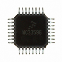
MC33596FJE Freescale Semiconductor, MC33596FJE Datasheet - Page 31

MC33596FJE
Manufacturer Part Number
MC33596FJE
Description
IC RECEIVER UHF PLL TUNED 32LQFP
Manufacturer
Freescale Semiconductor
Type
Receiverr
Datasheet
1.MC33596FCAE.pdf
(70 pages)
Specifications of MC33596FJE
Frequency
304, 315, 426, 434, 868 & 915MHz
Sensitivity
-104dBm
Data Rate - Maximum
22.4 kBaud
Modulation Or Protocol
FSK, OOK
Applications
General Data Transfer
Current - Receiving
10.3mA
Data Interface
PCB, Surface Mount
Antenna Connector
PCB, Surface Mount
Voltage - Supply
2.7 V ~ 3.6 V, 4.5 V ~ 5.5 V
Operating Temperature
-40°C ~ 85°C
Package / Case
32-LQFP
Operating Frequency
915 MHz
Operating Supply Voltage
3.3 V or 5 V
Maximum Operating Temperature
+ 85 C
Minimum Operating Temperature
- 40 C
Mounting Style
SMD/SMT
Operating Temperature (min)
-40C
Operating Temperature (max)
85C
Operating Temperature Classification
Industrial
Modulation Type
FSK/OOK
Package Type
LQFP
Operating Supply Voltage (min)
2.7V
Lead Free Status / RoHS Status
Lead free / RoHS Compliant
Features
-
Memory Size
-
Lead Free Status / Rohs Status
Lead free / RoHS Compliant
Available stocks
Company
Part Number
Manufacturer
Quantity
Price
Part Number:
MC33596FJE
Manufacturer:
FREESCALE
Quantity:
20 000
Part Number:
MC33596FJER2
Manufacturer:
FREESCALE
Quantity:
20 000
15.1.1 Direct Switch Control
The conditions to enter direct switch control are:
By simply writing BANKA and BANKB, the active bank will be defined:
The defined bank is active after exiting the configuration mode, in other words, CONFB line goes high.
The direct switch control should be used when:
15.1.2 Strobe Pin Switch Control
The conditions to enter strobe pin switch control are:
By simply writing BANKA and BANKB, the active banks will be defined.
The strobe pin will control the off/on state of the MC33596. The various available sequences are described
in the following subsections.
15.1.2.1 BANKA = X, BANKB = 0
If strobe pin is 1, configuration is defined by Bank A, BANKS = 1.
If strobe pin is 0, MC33596 configuration is OFF.
If a message is received during State A, current state remains State A up to end of message.
Freescale Semiconductor
Strobe Pin
State A
•
•
•
•
•
•
•
BANKA
BANKA
Strobe pin = V
SOE bit = 0
X
When the strobe oscillator cannot be used to define the switch timing (for example, not periodic)
When strobe pin use is not possible (no sleep mode between the two configurations)
No automatic switching is required and MCU SPI access is possible
Strobe pin: controlled by MCU I/O port
SOE bit = 0
X
0
1
0
1
BANKB
BANKB
0
1
1
0
1
1
OFF
Bank A is active
Bank B is active
Not allowed in direct switch control
Bank A is active
Bank B is active
Bank A and Bank B are both active, configuration will toggle at each wakeup
CC
MC33596 Data Sheet, Rev. 4
State A
OFF
Configuration Switching
31


