ATMEGA64RZAV-10PU Atmel, ATMEGA64RZAV-10PU Datasheet - Page 6
ATMEGA64RZAV-10PU
Manufacturer Part Number
ATMEGA64RZAV-10PU
Description
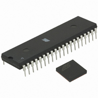
MCU ATMEGA644/AT86RF230 40-DIP
Manufacturer
Atmel
Series
ATMEGAr
Datasheets
1.ATMEGA644-20MU.pdf
(23 pages)
2.ATMEGA644-20MU.pdf
(376 pages)
3.AT86RF230-ZU.pdf
(98 pages)
Specifications of ATMEGA64RZAV-10PU
Frequency
2.4GHz
Modulation Or Protocol
802.15.4 Zigbee
Power - Output
3dBm
Sensitivity
-101dBm
Voltage - Supply
1.8 V ~ 3.6 V
Data Interface
PCB, Surface Mount
Memory Size
64kB Flash, 2kB EEPROM, 4kB RAM
Antenna Connector
PCB, Surface Mount
Package / Case
40-DIP (0.600", 15.24mm)
Wireless Frequency
2.4 GHz
Interface Type
JTAG, SPI
Output Power
3 dBm
For Use With
ATSTK600-TQFP32 - STK600 SOCKET/ADAPTER 32-TQFPATAVRISP2 - PROGRAMMER AVR IN SYSTEMATSTK500 - PROGRAMMER AVR STARTER KIT
Lead Free Status / RoHS Status
Lead free / RoHS Compliant
Operating Temperature
-
Applications
-
Data Rate - Maximum
-
Current - Transmitting
-
Current - Receiving
-
Lead Free Status / Rohs Status
Lead free / RoHS Compliant
For Use With/related Products
ATmega64


Table 4-2. Comments on Analog and RF Pins
4.3 Digital Pins
4.3.1 Driver Strength Settings of Digital Output Pins
6
Pin
RFP/RFN
XTAL1/XTAL2
AT86RF230
Condition
VDC = 0.9V (TX)
VDC = 20 mV (RX) at both pins
CPAR = 3 pF
VDC = 0.9V at both pins
In receive mode, the RF input provides a low-impedance path to ground when transistor
M0 (see Figure 4-1) pulls the inductor center tap to ground. A DC voltage drop of 20 mV
across the on-chip inductor can be measured at the RF pins.
In transmit mode, a control loop provides a common-mode voltage of 0.9V. Transistor
M0 is off, allowing the PA to set the common-mode voltage. The common-mode
capacitance at each pin to ground shall be < 30 pF to ensure the stability of this
common-mode feedback loop.
XTAL1, XTAL2
The pin XTAL1 is the input of the reference oscillator amplifier (XOSC), XTAL2 is the
output. A detailed description of the crystal oscillator setup and the related
XTAL1/XTAL2 pin configuration can be found in section 9.6.
When using an external clock reference signal, XTAL1 shall be used as input pin. For
further details refer to section 9.6.3.
The digital interface of the AT86RF230 compromises pins SEL , SCLK, MOSI and
MISO forming the serial peripheral interface (SPI) and pins CLKM, IRQ, SLP_TR and
The digital radio transceiver interface is described in detail in section 6.
The driver strength of the digital output pins (MISO, IRQ) and CLKM pin can be
configured by register 0x03 (TRX_CTRL_0) as described in Table 4-3.
The capacitive load should be as small as possible and not larger than 50 pF when
using the 2 mA minimum driver strength setting. Generally, the output driver strength
should be adjusted to the lowest possible value in order to keep the current
consumption and the emission of digital signal harmonics low.
Table 4-3. Digital Output Driver Configuration
RST used as additional control signal between radio transceiver and microcontroller.
Pin
MISO, IRQ
CLKM
Default Driver Strength
2 mA
4 mA
Recommendation/Comment
AC-coupling is required if an antenna with a DC path to ground is used.
Serial capacitance must be < 30 pF.
Parasitic capacitance (CPAR) of the pins must be considered as additional
load capacitance to the crystal.
Comment
Adjustable to 2 mA, 4 mA, 6 mA and 8 mA
Adjustable to 2 mA, 4 mA, 6 mA and 8 mA
5131E-MCU Wireless-02/09
Related parts for ATMEGA64RZAV-10PU
Image
Part Number
Description
Manufacturer
Datasheet
Request
R

Part Number:
Description:
DEV KIT FOR AVR/AVR32
Manufacturer:
Atmel
Datasheet:

Part Number:
Description:
INTERVAL AND WIPE/WASH WIPER CONTROL IC WITH DELAY
Manufacturer:
ATMEL Corporation
Datasheet:
Part Number:
Description:
Low-Voltage Voice-Switched IC for Hands-Free Operation
Manufacturer:
ATMEL Corporation
Datasheet:
Part Number:
Description:
MONOLITHIC INTEGRATED FEATUREPHONE CIRCUIT
Manufacturer:
ATMEL Corporation
Datasheet:
Part Number:
Description:
AM-FM Receiver IC U4255BM-M
Manufacturer:
ATMEL Corporation
Datasheet:
Part Number:
Description:
Monolithic Integrated Feature Phone Circuit
Manufacturer:
ATMEL Corporation
Datasheet:
Part Number:
Description:
Multistandard Video-IF and Quasi Parallel Sound Processing
Manufacturer:
ATMEL Corporation
Datasheet:
Part Number:
Description:
High-performance EE PLD
Manufacturer:
ATMEL Corporation
Datasheet:
Part Number:
Description:
8-bit Flash Microcontroller
Manufacturer:
ATMEL Corporation
Datasheet:
Part Number:
Description:
2-Wire Serial EEPROM
Manufacturer:
ATMEL Corporation
Datasheet: