ATMEGA64RZAV-10PU Atmel, ATMEGA64RZAV-10PU Datasheet - Page 62
ATMEGA64RZAV-10PU
Manufacturer Part Number
ATMEGA64RZAV-10PU
Description
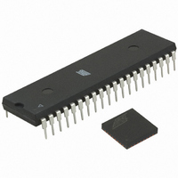
MCU ATMEGA644/AT86RF230 40-DIP
Manufacturer
Atmel
Series
ATMEGAr
Datasheets
1.ATMEGA644-20MU.pdf
(23 pages)
2.ATMEGA644-20MU.pdf
(376 pages)
3.AT86RF230-ZU.pdf
(98 pages)
Specifications of ATMEGA64RZAV-10PU
Frequency
2.4GHz
Modulation Or Protocol
802.15.4 Zigbee
Power - Output
3dBm
Sensitivity
-101dBm
Voltage - Supply
1.8 V ~ 3.6 V
Data Interface
PCB, Surface Mount
Memory Size
64kB Flash, 2kB EEPROM, 4kB RAM
Antenna Connector
PCB, Surface Mount
Package / Case
40-DIP (0.600", 15.24mm)
Wireless Frequency
2.4 GHz
Interface Type
JTAG, SPI
Output Power
3 dBm
For Use With
ATSTK600-TQFP32 - STK600 SOCKET/ADAPTER 32-TQFPATAVRISP2 - PROGRAMMER AVR IN SYSTEMATSTK500 - PROGRAMMER AVR STARTER KIT
Lead Free Status / RoHS Status
Lead free / RoHS Compliant
Operating Temperature
-
Applications
-
Data Rate - Maximum
-
Current - Transmitting
-
Current - Receiving
-
Lead Free Status / Rohs Status
Lead free / RoHS Compliant
For Use With/related Products
ATmega64


9.4 Voltage Regulators (AVREG, DVREG)
9.4.1 Overview
62
AT86RF230
the SPI transfer rate shall be lower than 250 Kbit/s to ensure no TRX_UR interrupt
occurs.
Note, during the Frame Buffer read access the TRX_UR interrupt is first valid 64 µs
after the RX_START interrupt. The occurrence of the interrupt can be disregarded when
reading the first byte of the Frame Buffer between 32 µs and 64 µs after the
RX_START interrupt.
If a received frame upload is delayed and during the upload process a new frame is
received, a TRX_UR and an RX_START interrupt occurs. Even so, the old frame data
can be read, if the SPI data rate is higher than the effective over air data rate. A
minimum SPI clock rate of 1 MHz is recommended in this special case. Finally it is
required to check the uploaded frame data integrity by a FCS using the microcontroller.
When writing data to the Frame Buffer during frame transmission, the SPI transfer rate
shall be higher than 250 Kbit/s to ensure no TRX_UR interrupt occurs. The first byte of
the PSDU data must be available in the Frame Buffer before SFD transmission has
been completed, which takes 176 µs (16 µs PA ramp up + 128 µs preamble
transmission + 32 µs SFD transmission) from the rising edge of SLP_TR pin (see
Figure 7-2).
The main features of the Voltage Regulator modules are:
• Bandgap stabilized 1.8V supply for analog and digital domain.
• Low dropout (LDO) voltage regulator
• Configurable for usage of external voltage regulator
The internal voltage regulators supply the low voltage domains of the AT86RF230. The
AVREG provides the regulated 1.8V supply voltage for the analog section and the
DVREG supplies the 1.8V supply voltage for the digital section. A simplified schematic
of the internal voltage regulator is shown in Figure 9-2.
Figure 9-2. Simplified Schematic of AVREG/DVREG
reference
Bandgap
voltage
1.25V
DEVDD / EVDD
DVDD / AVDD
5131E-MCU Wireless-02/09
Related parts for ATMEGA64RZAV-10PU
Image
Part Number
Description
Manufacturer
Datasheet
Request
R

Part Number:
Description:
DEV KIT FOR AVR/AVR32
Manufacturer:
Atmel
Datasheet:

Part Number:
Description:
INTERVAL AND WIPE/WASH WIPER CONTROL IC WITH DELAY
Manufacturer:
ATMEL Corporation
Datasheet:
Part Number:
Description:
Low-Voltage Voice-Switched IC for Hands-Free Operation
Manufacturer:
ATMEL Corporation
Datasheet:
Part Number:
Description:
MONOLITHIC INTEGRATED FEATUREPHONE CIRCUIT
Manufacturer:
ATMEL Corporation
Datasheet:
Part Number:
Description:
AM-FM Receiver IC U4255BM-M
Manufacturer:
ATMEL Corporation
Datasheet:
Part Number:
Description:
Monolithic Integrated Feature Phone Circuit
Manufacturer:
ATMEL Corporation
Datasheet:
Part Number:
Description:
Multistandard Video-IF and Quasi Parallel Sound Processing
Manufacturer:
ATMEL Corporation
Datasheet:
Part Number:
Description:
High-performance EE PLD
Manufacturer:
ATMEL Corporation
Datasheet:
Part Number:
Description:
8-bit Flash Microcontroller
Manufacturer:
ATMEL Corporation
Datasheet:
Part Number:
Description:
2-Wire Serial EEPROM
Manufacturer:
ATMEL Corporation
Datasheet: