ATMEGA64RZAV-10PU Atmel, ATMEGA64RZAV-10PU Datasheet - Page 69
ATMEGA64RZAV-10PU
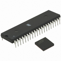
Manufacturer Part Number
ATMEGA64RZAV-10PU
Description
MCU ATMEGA644/AT86RF230 40-DIP
Manufacturer
Atmel
Series
ATMEGAr
Datasheets
1.ATMEGA644-20MU.pdf
(23 pages)
2.ATMEGA644-20MU.pdf
(376 pages)
3.AT86RF230-ZU.pdf
(98 pages)
Specifications of ATMEGA64RZAV-10PU
Frequency
2.4GHz
Modulation Or Protocol
802.15.4 Zigbee
Power - Output
3dBm
Sensitivity
-101dBm
Voltage - Supply
1.8 V ~ 3.6 V
Data Interface
PCB, Surface Mount
Memory Size
64kB Flash, 2kB EEPROM, 4kB RAM
Antenna Connector
PCB, Surface Mount
Package / Case
40-DIP (0.600", 15.24mm)
Wireless Frequency
2.4 GHz
Interface Type
JTAG, SPI
Output Power
3 dBm
For Use With
ATSTK600-TQFP32 - STK600 SOCKET/ADAPTER 32-TQFPATAVRISP2 - PROGRAMMER AVR IN SYSTEMATSTK500 - PROGRAMMER AVR STARTER KIT
Lead Free Status / RoHS Status
Lead free / RoHS Compliant
Operating Temperature
-
Applications
-
Data Rate - Maximum
-
Current - Transmitting
-
Current - Receiving
-
Lead Free Status / Rohs Status
Lead free / RoHS Compliant
For Use With/related Products
ATmega64


9.6.5 Register Description
5131E-MCU Wireless-02/09
Bit
0x03
Read/Write
Reset value
Bit
0x03
Read/Write
Reset value
To reduce power consumption and spurious emissions, it is recommended to turn off
the CLKM clock when not in use or to reduce its driver strength to a minimum, refer to
section 4.3.
Note:
During reset procedure, see section 7.1.4.2, register bits CLKM_CTRL are shadowed.
Although the clock setting of CLKM remains after reset, a read access to register bits
CLKM_CTRL delivers the reset value 1. For that reason it is recommended to write the
previous configuration (before reset) to the CLKM_CTRL to align the radio transceiver
behavior and register configuration. Otherwise the CLKM clock rate is set back to the
reset value (1 MHz) after the next SLEEP cycle.
For example if the CLKM clock rate is configured to 16 MHz the CLKM rate remains at
16 MHz after a reset, however the register bits CLKM_CTRL are set back to 1. Since
CLKM_SHA_SEL reset value is 1, the CLKM clock rate would change to 1 MHz after
the next SLEEP cycle if the CLKM_CTRL setting is not updated.
Register 0x03 (TRX_CTRL_0)
The TRX_CTRL_0 register controls the drive current of the digital output pads and the
CLKM clock rate.
• Bit [7:6] – PAD_IO
Refer to in section 4.3.3.
• Bit [5:6] – PAD_IO_CLKM
The register bits PAD_IO_CLKM set the output driver current of pin CLKM.
Table 9-9. CLKM Driver Strength
• Bit 3 – CLKM_SHA_SEL
The register bit CLKM_SHA_SEL defines the commencement of the CLKM clock rate
modifications when changing register bits CLKM_CTRL.
Table 9-10. Commencement of CLKM Clock Rate Modification
Register Bit
PAD_IO_CLKM
Register Bit
CLKM_SHA_SEL
CLKM_SHA_SEL
R/W
R/W
7
0
3
1
PAD_IO
Value
Value
0
1
2
3
0
R/W
R/W
6
0
2
0
Description
2 mA
4 mA
6 mA
8 mA
Description
CLKM clock rate changes immediately
CLKM_CTRL
R/W
R/W
5
0
1
0
PAD_IO_CLKM
R/W
R/W
AT86RF230
4
1
0
1
TRX_CTRL_0
TRX_CTRL_0
69
Related parts for ATMEGA64RZAV-10PU
Image
Part Number
Description
Manufacturer
Datasheet
Request
R

Part Number:
Description:
DEV KIT FOR AVR/AVR32
Manufacturer:
Atmel
Datasheet:

Part Number:
Description:
INTERVAL AND WIPE/WASH WIPER CONTROL IC WITH DELAY
Manufacturer:
ATMEL Corporation
Datasheet:
Part Number:
Description:
Low-Voltage Voice-Switched IC for Hands-Free Operation
Manufacturer:
ATMEL Corporation
Datasheet:
Part Number:
Description:
MONOLITHIC INTEGRATED FEATUREPHONE CIRCUIT
Manufacturer:
ATMEL Corporation
Datasheet:
Part Number:
Description:
AM-FM Receiver IC U4255BM-M
Manufacturer:
ATMEL Corporation
Datasheet:
Part Number:
Description:
Monolithic Integrated Feature Phone Circuit
Manufacturer:
ATMEL Corporation
Datasheet:
Part Number:
Description:
Multistandard Video-IF and Quasi Parallel Sound Processing
Manufacturer:
ATMEL Corporation
Datasheet:
Part Number:
Description:
High-performance EE PLD
Manufacturer:
ATMEL Corporation
Datasheet:
Part Number:
Description:
8-bit Flash Microcontroller
Manufacturer:
ATMEL Corporation
Datasheet:
Part Number:
Description:
2-Wire Serial EEPROM
Manufacturer:
ATMEL Corporation
Datasheet: