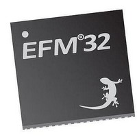
EFM32TG210F32 Energy Micro, EFM32TG210F32 Datasheet - Page 452

EFM32TG210F32
Manufacturer Part Number
EFM32TG210F32
Description
MCU 32BIT 32KB FLASH 32-QFN
Manufacturer
Energy Micro
Series
Tiny Geckor
Specifications of EFM32TG210F32
Core Processor
ARM® Cortex-M3™
Core Size
32-Bit
Speed
32MHz
Connectivity
EBI/EMI, I²C, IrDA, SmartCard, SPI, UART/USART
Peripherals
Brown-out Detect/Reset, DMA, POR, PWM, WDT
Number Of I /o
24
Program Memory Size
32KB (32K x 8)
Program Memory Type
FLASH
Ram Size
4K x 8
Voltage - Supply (vcc/vdd)
1.8 V ~ 3.8 V
Data Converters
A/D 4x12b, D/A 1x12b
Oscillator Type
External
Operating Temperature
-40°C ~ 85°C
Package / Case
32-VQFN Exposed Pad
Processor Series
EFM32
Core
ARM Cortex-M3
Data Bus Width
32 bit
Data Ram Size
32 KB
Interface Type
UART, I2C, SPI
Maximum Clock Frequency
32 MHz
Number Of Programmable I/os
17
Number Of Timers
1
Operating Supply Voltage
1.8 V to 3.8 V
Maximum Operating Temperature
+ 85 C
Mounting Style
SMD/SMT
Processor To Be Evaluated
EFM32TG210
Lead Free Status / RoHS Status
Lead free / RoHS Compliant
Eeprom Size
-
Lead Free Status / Rohs Status
Details
- Current page: 452 of 522
- Download datasheet (9Mb)
28.3.3 EM4 Retention
28.3.4 Alternate Functions
2010-12-21 - d0034_Rev0.90
Figure 28.5. EM4 Wake-up Logic
The pins used for EM4 wake-up must be configured as inputs using the GPIO_Px_MODEL/
GPIO_Px_MODEH register. If input is disabled, the wakeup polarity is low a false wakeup will happen
when entering EM4. Before going down to EM4, it is important to clear the wake-up logic by setting
the EM4WUCLR bitfield in the GPIO_EM4WUCMD register, which clears the complete wake-up logic,
including the GPIO_EM4WUCAUSE register. When the chip comes out of reset, it is possible to
determine what caused the reset by reading the RMU_RSTCAUSE register. If an em4 wake-up reset
occured, the EM4RST (indicating the chip was in EM4) and the EM4WU (indicating the EM4 wake-
up reset) bits should be set. It is possible to determine which pin caused the reset by reading the
GPIO_EM4WUCAUSE register. The mapping between pins and the bits in the GPIO_EM4WUEN,
GPIO_EM4WUPOL, and GPIO_EM4WUCAUSE registers are described in Table 28.2 (p. 452)
Table 28.2. EM4 WU Register bits to pin mapping
It is possible to enable retention of output enable, output value and pull enable when in EM4. EM4
retention also makes it possible to wake up from EM4 on pin reset as described in Section 28.3.2 (p.
451) EM4 retention can be enabled by setting the EM4RET field in GPIO_CTRL register before going
down in EM4.
Alternate functions are connections to pins from Timers, USARTs etc. These modules contain route
registers, where the pin connections are enabled. In addition, these registers contain a location bit
field, which configures which pins the outputs of that module will be connected to if they are enabled.
If an alternate signal output is enabled for a pin and output is enabled for the pin, the alternate
function’s output data and output enable signals override the data output and output enable signals
from the GPIO. However, the pin configuration stays as set in GPIO_Px_MODEL, GPIO_Px_MODEH
and GPIO_Px_DOUT registers. I.e. the pin configuration must be set to output enable in GPIO for a
peripheral to be able to use the pin as an output.
Wake-up Registers Bits
bit 0
bit 1
bit 2
bit 3
bit 4
bit 5
GPIO_EM4WUPOL
GPIO_CMD
GPIO_EM4WUCAUSE
Wake-up Logic
...the world's most energy friendly microcontrollers
452
Pin
A0
A6
C9
F1
F2
E13
GPIO_EM4WUEN
Wake-up request
www.energymicro.com
Related parts for EFM32TG210F32
Image
Part Number
Description
Manufacturer
Datasheet
Request
R

Part Number:
Description:
KIT STARTER EFM32 GECKO
Manufacturer:
Energy Micro
Datasheet:

Part Number:
Description:
KIT DEV EFM32 GECKO LCD SUPPORT
Manufacturer:
Energy Micro
Datasheet:

Part Number:
Description:
BOARD PROTOTYPING FOR EFM32
Manufacturer:
Energy Micro
Datasheet:

Part Number:
Description:
KIT DEVELOPMENT EFM32 GECKO
Manufacturer:
Energy Micro
Datasheet:

Part Number:
Description:
MCU, MPU & DSP Development Tools TG840 Sample Kit
Manufacturer:
Energy Micro
Datasheet:

Part Number:
Description:
MCU, MPU & DSP Development Tools TG Starter Kit
Manufacturer:
Energy Micro
Datasheet:

Part Number:
Description:
MCU, MPU & DSP Development Tools TG108 Sample Kit
Manufacturer:
Energy Micro

Part Number:
Description:
MCU, MPU & DSP Development Tools TG210 Sample Kit
Manufacturer:
Energy Micro
Datasheet:

Part Number:
Description:
MCU, MPU & DSP Development Tools TG822 Sample Kit
Manufacturer:
Energy Micro
Datasheet:

Part Number:
Description:
MCU, MPU & DSP Development Tools TG230 Sample Kit
Manufacturer:
Energy Micro

Part Number:
Description:
SAMPLE KIT (SMALL BOX - CONTAINING 2 DEVICES)
Manufacturer:
Energy Micro

Part Number:
Description:
SAMPLE KIT (SMALL BOX - CONTAINING 2 DEVICES)
Manufacturer:
Energy Micro


