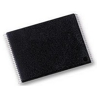
H27UF081G1M-TPCB HYNIX SEMICONDUCTOR, H27UF081G1M-TPCB Datasheet - Page 14

H27UF081G1M-TPCB
Manufacturer Part Number
H27UF081G1M-TPCB
Description
IC, MEMORY, FLASH NAND 1GB, TSOP48
Manufacturer
HYNIX SEMICONDUCTOR
Datasheet
1.H27UF081G1M-TPCB.pdf
(39 pages)
Specifications of H27UF081G1M-TPCB
Access Time
45ns
Supply Voltage Range
2.7V To 3.6V
Memory Case Style
TSOP
No. Of Pins
48
Operating Temperature Range
0°C To +70°C
Base Number
27
Interface
Serial
Logic
RoHS Compliant
Package / Case
TSOP
Memory Type
Flash - NAND
Memory Configuration
128M X 8
Rohs Compliant
Yes
Memory Size
1Gbit
Preliminary
HY27US(08/16)1G1M Series
1Gbit (128Mx8bit / 64Mx16bit) NAND Flash
4. OTHER FEATURES
4.1 Data Protection & Power on/off Sequence
The device is designed to offer protection from any involuntary program/erase during power-transitions. An internal
voltage detector disables all functions whenever Vcc is below about 2.0V(3.3V device). WP pin provides hardware pro-
tection and is recommended to be kept at VIL during power-up and power-down. A recovery time of minimum 10us is
required before internal circuit gets ready for any command sequences as shown in Figure 20. The two-step command
sequence for program/erase provides additional software protection.
If the power is dropped during the ready read/write/erase operation, Power protection function may not guaranteed
the data. Power protection function is only available during the power on/off sequence.
4.2 Ready/Busy.
The device has a Ready/Busy output that provides method of indicating the completion of a page program, erase,
copy-back, cache program and random read completion. The R/B pin is normally high and goes to low when the device
is busy (after a reset, read, program, erase operation). It returns to high when the internal controller has finished the
operation. The pin is an open-drain driver thereby allowing two or more R/B outputs to be Or-tied. Because pull-up
resistor value is related to tr(R/B) and current drain during busy (Ibusy), an appropriate value can be obtained with
the following reference chart (Fig 21). Its value can be determined by the following guidance.
4.3 Power-On Auto-Read
The device is designed to offer automatic reading of the first page without command and address input sequence dur-
ing power-on.
An internal voltage detector enables auto-page read functions when Vcc reaches about 1.8V.
Serial access may be done after power-on without latency. Power-On Auto Read mode is available only on 3.3V device.
Rev 0.2 / May. 2007
14


