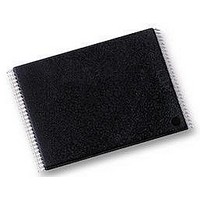
H27UF081G1M-TPCB HYNIX SEMICONDUCTOR, H27UF081G1M-TPCB Datasheet - Page 34

H27UF081G1M-TPCB
Manufacturer Part Number
H27UF081G1M-TPCB
Description
IC, MEMORY, FLASH NAND 1GB, TSOP48
Manufacturer
HYNIX SEMICONDUCTOR
Datasheet
1.H27UF081G1M-TPCB.pdf
(39 pages)
Specifications of H27UF081G1M-TPCB
Access Time
45ns
Supply Voltage Range
2.7V To 3.6V
Memory Case Style
TSOP
No. Of Pins
48
Operating Temperature Range
0°C To +70°C
Base Number
27
Interface
Serial
Logic
RoHS Compliant
Package / Case
TSOP
Memory Type
Flash - NAND
Memory Configuration
128M X 8
Rohs Compliant
Yes
Memory Size
1Gbit
Preliminary
HY27US(08/16)1G1M Series
1Gbit (128Mx8bit / 64Mx16bit) NAND Flash
Bad Block Management
Devices with Bad Blocks have the same quality level and the same AC and DC characteristics as devices where all the blocks are valid.
A Bad Block does not affect the performance of valid blocks because it is isolated from the bit line and common source line by a
select transistor. The devices are supplied with all the locations inside valid blocks erased(FFh/FFFFh).
The Bad Block Information is written prior to shipping. Any block where the 6th Byte/ 1st Word in the spare area of the 1st or 2nd
page (if the 1st page is Bad) does not contain FFh/FFFFh is a Bad Block. The Bad Block Information must be read before any erase is
attempted as the Bad Block Information may be erased. For the system to be able to recognize the Bad Blocks based on the original
information it is recommended to create a Bad Block table following the flowchart shown in Figure 26. The 1st block, which is placed
on 00h block address is guaranteed to be a valid block.
Block Replacement
Over the lifetime of the device additional Bad Blocks may develop. In this case the block has to be replaced by copying the data to a
valid block. These additional Bad Blocks can be identified as attempts to program or erase them will give errors in the Status Regis-
ter.
As the failure of a page program operation does not affect the data in other pages in the same block, the block can be replaced by
re-programming the current data and copying the rest of the replaced block to an available valid block.
The Copy Back Program command can be used to copy the data to a valid block.
See the “Copy Back Program” section for more details.
Refer to Table 16 for the recommended procedure to follow if an error occurs during an operation.
Recommended Procedure
Operation
Erase
Block Replacement
Program
Block Replacement or ECC (with 4bit/528byte)
Read
ECC (with 4bit/528byte)
Table 16: Block Failure
Figure 26: Bad Block Management Flowchart
Rev 0.2 / May. 2007
34


