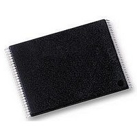
H27UF081G1M-TPCB HYNIX SEMICONDUCTOR, H27UF081G1M-TPCB Datasheet - Page 20

H27UF081G1M-TPCB
Manufacturer Part Number
H27UF081G1M-TPCB
Description
IC, MEMORY, FLASH NAND 1GB, TSOP48
Manufacturer
HYNIX SEMICONDUCTOR
Datasheet
1.H27UF081G1M-TPCB.pdf
(39 pages)
Specifications of H27UF081G1M-TPCB
Access Time
45ns
Supply Voltage Range
2.7V To 3.6V
Memory Case Style
TSOP
No. Of Pins
48
Operating Temperature Range
0°C To +70°C
Base Number
27
Interface
Serial
Logic
RoHS Compliant
Package / Case
TSOP
Memory Type
Flash - NAND
Memory Configuration
128M X 8
Rohs Compliant
Yes
Memory Size
1Gbit
Rev 0.2 / May. 2007
IO
0
1
2
3
4
5
6
7
DEVICE IDENTIFIER CYCLE
HY27US081G1M
HY27US161G1M
Part Number
Write Protect
Ready/Busy
Ready/Busy
Pass / Fail
Program
Pagae
2nd
3rd
4th
1st
NA
NA
NA
NA
Voltage
3.3V
3.3V
Bus Width
Table 14: Device Identifier Coding
Write Protect
Ready/Busy
Ready/Busy
Table 13: Status Register Coding
Pass / Fail
Table 15: Read ID Data Table
Block
Erase
x16
x8
Internal chip number, cell Type, Number of simultaneously Programmed
NA
NA
NA
NA
1Gbit (128Mx8bit / 64Mx16bit) NAND Flash
(Manufacture Code)
Page size, Spare size, Block size, Organization
1st cycle
ADh
ADh
Write Protect
Ready/Busy
Ready/Busy
Read
NA
NA
NA
NA
NA
Manufacturer Code
Device Identifier
DESCRIPTION
HY27US(08/16)1G1M Series
pages
(Device Code)
2nd cycle
79h
74h
Busy: ‘0’ Ready’: ‘1’
Active: ‘0’ Idle: ‘1’
Not Protected: ‘1’
Pass: ‘0’ Fail: ‘1’
Protected: ‘0’
CODING
3rd Cycle 4th Cycle
-
-
-
-
A5h
A5h
Preliminary
00h
00h
20


