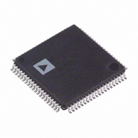
AD9980KSTZ-80 Analog Devices Inc, AD9980KSTZ-80 Datasheet - Page 30

AD9980KSTZ-80
Manufacturer Part Number
AD9980KSTZ-80
Description
IC,Data Acquisition Signal Conditioner,3-CHANNEL,8-BIT,CMOS,QFP,80PIN,PLASTIC
Manufacturer
Analog Devices Inc
Datasheet
1.AD9980KSTZ-80.pdf
(44 pages)
Specifications of AD9980KSTZ-80
Applications
Video
Interface
Analog
Voltage - Supply
3.13 V ~ 3.47 V
Package / Case
80-LQFP
Mounting Type
Surface Mount
Lead Free Status / RoHS Status
Lead free / RoHS Compliant
For Use With
AD9980/PCBZ - KIT EVALUATION AD9980
Lead Free Status / RoHS Status
Lead free / RoHS Compliant
Available stocks
Company
Part Number
Manufacturer
Quantity
Price
Company:
Part Number:
AD9980KSTZ-80
Manufacturer:
ADI
Quantity:
830
Company:
Part Number:
AD9980KSTZ-80
Manufacturer:
Analog Devices Inc
Quantity:
10 000
Part Number:
AD9980KSTZ-80
Manufacturer:
ADI/亚德诺
Quantity:
20 000
AD9980
0x12
Table 16. Active Hsync Source Override
Override
0
1
0x12
Table 17. Active Hsync Select Settings
0x12
Table 18. Hsync Input Polarity Override Settings
Override Bit
0
1
0x12
Table 19. Hsync Input Polarity Settings
Hsync Polarity Bit
0
1
0x12
Select
0
1
7
This is the active Hsync override. Setting this to 0
allows the chip to determine the active Hsync source.
Setting it to 1 uses Bit 6 of Register 0x12 to determine
the active Hsync source. Power-up default value is 0.
6
This bit selects the source of the Hsync for PLL and
sync processing only if Bit 7 of Register 0x12 is set to 1
or if both syncs are active. Setting this bit to 0 specifies
the Hsync from the input pin. Setting it to 1 selects
Hsync from SOG. Power-up default is 0.
5
This bit sets whether the chip selects the Hsync input
polarity or if it is specified. Setting this bit to 0 allows
the chip to automatically select the polarity of the
input Hsync. Setting this bit to 1 indicates that Bit 4 of
Register 0x12 specifies the polarity. Power-up default
is 0.
4
If Bit 5 of Register 0x12 is 1, the value of this bit
specifies the polarity of the input Hsync. Setting this
bit to 0 indicates an active low Hsync; setting this bit
to 1 indicates an active high Hsync. Power-up default
is 1.
3
This bit sets the polarity of the Hsync output. Setting
this bit to 0 sets the Hsync output to active low. Setting
this bit to 1 sets the Hsync output to active high.
Power-up default setting is 1.
Hsync Source Override
Hsync Source
Hsync Input Polarity Override
Input Hsync Polarity
Hsync Output Polarity
Result
Hsync Source determined by chip
Hsync Source determined by user
Register 0x12, Bit 6
Result
Hsync Input
Hsync from SOG
Result
Hsync Polarity Determined by Chip
Hsync Polarity Determined by User
Register 0x12, Bit 4
Result
Hsync Input Polarity is Negative
Hsync Input Polarity is Positive
Rev. 0 | Page 30 of 44
Table 20. Hsync Output Polarity Settings
Hsync Output
Polarity Bit
0
1
0x13
VSYNC CONTROLS
0x14
Table 21. Active Vsync Source Override
Override
0
1
0x14
Table 22. Active Vsync Select Settings
Select
0
1
0x14
Table 23. Vsync Input Polarity Override Settings
Override Bit
0
1
7:0
An 8-bit register that sets the duration of the Hsync
output pulse. The leading edge of the Hsync output is
triggered by the internally-generated, phase-adjusted
PLL feedback clock. The AD9980 then counts a
number of pixel clocks equal to the value in this
register. This triggers the trailing edge of the Hsync
output, which is also phase-adjusted.
7
This is the active Vsync override. Setting this to 0
allows the chip to determine the active Vsync source.
Setting it to 1 uses Bit 6 of Register 0x14 to determine
the active Vsync source. Power-up default value is 0.
6
This bit selects the source of Vsync for sync
processing only if Bit 7 of Register 0x14 is set to 1.
Setting Bit 6 to 0 specifies Vsync from the input pin.
Setting it to 1 selects Vsync from the sync separator.
Power-up default is 0.
5
This bit sets whether the chip selects the Vsync input
polarity or if it is specified. Setting this bit to 0 allows
the chip to automatically select the polarity of the
input Vsync. Setting this bit to 1 indicates that Bit 4 of
Register 0x14 specifies the polarity. Power-up default
is 0.
Result
Hsync Output Polarity is Negative
Hsync Output Polarity is Positive
Result
Vsync source determined by chip
Vsync source determined by user
Register 0x14, Bit 6
Result
Vsync input
Vsync from sync separator
Result
Vsync polarity determined by chip
Vsync polarity determined by user
Register 0x14, Bit 4
Vsync Input Polarity Override
Hsync Duration
Vsync Source Override
Vsync Source
Preliminary Technical Data


