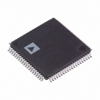
AD9980KSTZ-80 Analog Devices Inc, AD9980KSTZ-80 Datasheet - Page 31

AD9980KSTZ-80
Manufacturer Part Number
AD9980KSTZ-80
Description
IC,Data Acquisition Signal Conditioner,3-CHANNEL,8-BIT,CMOS,QFP,80PIN,PLASTIC
Manufacturer
Analog Devices Inc
Datasheet
1.AD9980KSTZ-80.pdf
(44 pages)
Specifications of AD9980KSTZ-80
Applications
Video
Interface
Analog
Voltage - Supply
3.13 V ~ 3.47 V
Package / Case
80-LQFP
Mounting Type
Surface Mount
Lead Free Status / RoHS Status
Lead free / RoHS Compliant
For Use With
AD9980/PCBZ - KIT EVALUATION AD9980
Lead Free Status / RoHS Status
Lead free / RoHS Compliant
Available stocks
Company
Part Number
Manufacturer
Quantity
Price
Company:
Part Number:
AD9980KSTZ-80
Manufacturer:
ADI
Quantity:
830
Company:
Part Number:
AD9980KSTZ-80
Manufacturer:
Analog Devices Inc
Quantity:
10 000
Part Number:
AD9980KSTZ-80
Manufacturer:
ADI/亚德诺
Quantity:
20 000
0x14
Table 24. Vsync Input Polarity Settings
Override Bit
0
1
0x14
Table 25. Vsync Output Polarity Settings
Vsync Output
Polarity Bit
0
1
0x14
Table 26. Vsync Filter Enable
Vsync Filter Bit
0
1
0x14
Table 27. Vsync Duration Enable
0x15
Vsync
Duration Bit
0
1
4
If Bit 5 of Register 0x14 is 1, the value of this bit
specifies the polarity of the input Vsync. Setting this
bit to 0 indicates an active low Vsync; setting this bit to
1 indicates an active high Vsync. Power-up default is 1.
3
This bit sets the polarity of the Hsync output. Setting
this bit to 0 sets the Hsync output to active low. Setting
this bit to 1 sets the Hsync output to active high.
Power-up default is 1.
2
This bit enables the Vsync filter allowing precise
placement of the Vsync with respect to the Hsync
and facilitating the correct operation of the
Hsyncs/Vsync count.
1
This enables the Vsync duration block, which is
designed to be used with the Vsync filter. Setting the
bit to 0 leaves the Vsync output duration unchanged.
Setting the bit to 1 sets the Vsync output duration
based on Register 0x15. Power-up duration is 0.
7:0
This is used to set the output duration of the Vsync,
and is designed to be used with the Vsync filter. This is
valid only if Register 0x14, Bit 1 is set to 1. Power-up
default is 10.
Input Vsync Polarity
Vsync Output Polarity
Vsync Filter Enable
Vsync Duration Enable
Vsync Duration
Result
Vsync input polarity is negative
Vsync input polarity is positive
Result
Vsync output polarity is negative
Vsync output polarity is positive
Result
Vsync filter disabled
Vsync filter enabled
Result
Vsync output duration is unchanged
Vsync output duration is set by Register 0x15
Rev. 0 | Page 31 of 44
COAST AND CLAMP CONTROLS
0x16
0x17
0x18
Table 28. Coast Source Selection Settings
0x18
Table 29. Coast Polarity Override Settings
Override Bit
0
1
0x18
Table 30. Coast Polarity Settings
Coast Polarity
Bit
0
1
Select
0
1
7:0
This register allows the internally generated Coast
signal to be applied prior to the Vsync signal. This is
necessary in cases where pre-equalization pulses are
present. The step size for this control is one Hsync
period. For Precoast to work correctly, it is necessary
for the Vsync filter (Register 0x14, Bit 2) and sync
processing filter (Register 0x20, Bit 1) both to be either
enabled or disabled. The power-up default is 00.
7:0
This register allows the internally generated Coast
signal to be applied following the Vsync signal. This is
necessary in cases where post equalization pulses are
present. The step size for this control is one Hsync
period. For Postcoast to work correctly, it is necessary
for the Vsync filter (Register 0x14, Bit 2) and sync
processing filter (Register 0x20, Bit 1) both to be either
enabled or disabled. The power-up default is 00.
7
This bit is used to select the active Coast source. The
choices are the COAST input pin or Vsync. If Vsync is
selected, the additional decision of using the Vsync
input pin or the output from the sync separator needs
to be made (Register 0x14, Bits [7: 6]).
6
This register is used to override the internal circuitry
that determines the polarity of the Coast signal going
into the PLL. The power-up default setting is 0.
5
This register sets the input Coast polarity when Bit 6
of Register 0x18 = 1. The power-up default setting is 1.
Precoast
Postcoast
Coast Source
Coast Polarity Override
Input Coast Polarity
Result
Vsync (internal Coast)
COAST input pin
Result
Coast polarity is negative
Coast polarity is positive
Result
Coast polarity determined by chip
Coast polarity determined by user
AD9980


