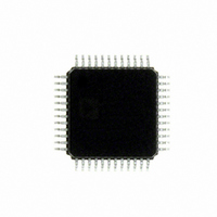
ADUC7060BSTZ32 Analog Devices Inc, ADUC7060BSTZ32 Datasheet - Page 31

ADUC7060BSTZ32
Manufacturer Part Number
ADUC7060BSTZ32
Description
DUAL 24-BIT AFE AND ARM 7 I.C
Manufacturer
Analog Devices Inc
Series
MicroConverter® ADuC7xxxr
Specifications of ADUC7060BSTZ32
Design Resources
4 mA-to-20 mA Loop-Powered Temperature Monitor Using ADuC7060/1 (CN0145) Low power, Long Range, ISM Wireless Measuring Node (CN0164)
Core Processor
ARM7
Core Size
16/32-Bit
Speed
10MHz
Connectivity
I²C, SPI, UART/USART
Peripherals
POR, PWM, Temp Sensor, WDT
Number Of I /o
14
Program Memory Size
32KB (16K x 16)
Program Memory Type
FLASH
Ram Size
4K x 8
Voltage - Supply (vcc/vdd)
2.375 V ~ 2.625 V
Data Converters
A/D 5x24b, 8x24b, D/A 1x14b
Oscillator Type
Internal
Operating Temperature
-40°C ~ 125°C
Package / Case
48-LQFP
Cpu Family
ADuC7xxx
Device Core
ARM7TDMI
Device Core Size
16/32Bit
Frequency (max)
10.24MHz
Interface Type
I2C/SPI/UART
Total Internal Ram Size
4KB
# I/os (max)
14
Number Of Timers - General Purpose
4
Operating Supply Voltage (typ)
2.5V
Operating Supply Voltage (max)
2.625V
Operating Supply Voltage (min)
2.375V
On-chip Adc
2(4-chx24-bit)
Instruction Set Architecture
RISC
Operating Temp Range
-40C to 125C
Operating Temperature Classification
Automotive
Mounting
Surface Mount
Pin Count
48
Package Type
LQFP
Package
48LQFP
Family Name
ADuC7xxx
Maximum Speed
10.24 MHz
Operating Supply Voltage
2.5 V
Data Bus Width
16|32 Bit
Number Of Programmable I/os
14
Number Of Timers
4
Lead Free Status / RoHS Status
Lead free / RoHS Compliant
Eeprom Size
-
Lead Free Status / Rohs Status
Compliant
Available stocks
Company
Part Number
Manufacturer
Quantity
Price
Company:
Part Number:
ADUC7060BSTZ32
Manufacturer:
CYPRESS
Quantity:
294
Company:
Part Number:
ADUC7060BSTZ32
Manufacturer:
ADI
Quantity:
315
Company:
Part Number:
ADUC7060BSTZ32
Manufacturer:
Analog Devices Inc
Quantity:
10 000
Part Number:
ADUC7060BSTZ32
Manufacturer:
ADI/亚德诺
Quantity:
20 000
Company:
Part Number:
ADUC7060BSTZ32-RL
Manufacturer:
Analog Devices Inc
Quantity:
10 000
Table 27. Flash/EE Base Address = 0xFFFF0E00
Address
0x0E00
0x0E04
0x0E08
0x0E0C
0x0E10
0x0E18
0x0E1C
0x0E20
Table 28. PWM Base Address = 0xFFFF0F80
Address
0x0F80
0x0F84
0x0F88
0x0F8C
0x0F90
0x0F94
0x0F98
0x0F9C
0x0FA0
0x0FA4
0x0FA8
0x0FAC
0x0FB0
0x0FB8
Name
PWMCON
PWM0COM0
PWM0COM1
PWM0COM2
PWM0LEN
PWM1COM0
PWM1COM1
PWM1COM2
PWM1LEN
PWM2COM0
PWM2COM1
PWM2COM2
PWM2LEN
PWMCLRI
Name
FEESTA
FEEMOD
FEECON
FEEDAT
FEEADR
FEESIGN
FEEPRO
FEEHIDE
Bytes
2
2
1
2
2
3
4
4
Bytes
2
2
2
2
2
2
2
2
2
2
2
2
2
2
R/W
Access
Type
R/W
R/W
R/W
R/W
R/W
R/W
R/W
R/W
R/W
R/W
R/W
R/W
R/W
W
Access
Type
R
R/W
R/W
R/W
R/W
R
R/W
Default Value
0x20
0x0000
0x07
0xXXXX
0x0000
0xFFFFFF
0x00000000
0xFFFFFFFF
Default Value
0x0012
0x0000
0x0000
0x0000
0x0000
0x0000
0x0000
0x0000
0x0000
0x0000
0x0000
0x0000
0x0000
0x0000
Rev. B | Page 31 of 108
Description
Flash/EE status MMR.
Flash/EE control MMR.
Flash/EE data MMR.
Flash/EE address MMR.
Flash/EE LFSR MMR.
Flash/EE protection MMR.
Flash/EE protection MMR.
Flash/EE control MMR.
Description
PWM control register. See the Pulse-Width Modulatorsection for full
details.
Compare Register 0 for PWM Output 0 and PWM Output 1.
Compare Register 1 for PWM Output 0 and PWM Output 1.
Compare Register 2 for PWM Output 0 and PWM Output 1.
Frequency control for PWM Output 0 and PWM Output 1.
Compare Register 0 for PWM Output 2 and PWM Output 3.
Compare Register 1 for PWM Output 2 and PWM Output 3.
Compare Register 2 for PWM Output 2 and PWM Output 3.
Frequency control for PWM Output 2 and PWM Output 3.
Compare Register 0 for PWM Output 4 and PWM Output 5.
Compare Register 1 for PWM Output 4 and PWM Output 5.
Compare Register 2 for PWM Output 4 and PWM Output 5.
Frequency control for PWM Output 4 and PWM Output 5.
PWM interrupt clear register. Writing any value to this register clears a
PWM interrupt source.
ADuC7060/ADuC7061


