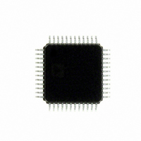
ADUC7060BSTZ32 Analog Devices Inc, ADUC7060BSTZ32 Datasheet - Page 91

ADUC7060BSTZ32
Manufacturer Part Number
ADUC7060BSTZ32
Description
DUAL 24-BIT AFE AND ARM 7 I.C
Manufacturer
Analog Devices Inc
Series
MicroConverter® ADuC7xxxr
Specifications of ADUC7060BSTZ32
Design Resources
4 mA-to-20 mA Loop-Powered Temperature Monitor Using ADuC7060/1 (CN0145) Low power, Long Range, ISM Wireless Measuring Node (CN0164)
Core Processor
ARM7
Core Size
16/32-Bit
Speed
10MHz
Connectivity
I²C, SPI, UART/USART
Peripherals
POR, PWM, Temp Sensor, WDT
Number Of I /o
14
Program Memory Size
32KB (16K x 16)
Program Memory Type
FLASH
Ram Size
4K x 8
Voltage - Supply (vcc/vdd)
2.375 V ~ 2.625 V
Data Converters
A/D 5x24b, 8x24b, D/A 1x14b
Oscillator Type
Internal
Operating Temperature
-40°C ~ 125°C
Package / Case
48-LQFP
Cpu Family
ADuC7xxx
Device Core
ARM7TDMI
Device Core Size
16/32Bit
Frequency (max)
10.24MHz
Interface Type
I2C/SPI/UART
Total Internal Ram Size
4KB
# I/os (max)
14
Number Of Timers - General Purpose
4
Operating Supply Voltage (typ)
2.5V
Operating Supply Voltage (max)
2.625V
Operating Supply Voltage (min)
2.375V
On-chip Adc
2(4-chx24-bit)
Instruction Set Architecture
RISC
Operating Temp Range
-40C to 125C
Operating Temperature Classification
Automotive
Mounting
Surface Mount
Pin Count
48
Package Type
LQFP
Package
48LQFP
Family Name
ADuC7xxx
Maximum Speed
10.24 MHz
Operating Supply Voltage
2.5 V
Data Bus Width
16|32 Bit
Number Of Programmable I/os
14
Number Of Timers
4
Lead Free Status / RoHS Status
Lead free / RoHS Compliant
Eeprom Size
-
Lead Free Status / Rohs Status
Compliant
Available stocks
Company
Part Number
Manufacturer
Quantity
Price
Company:
Part Number:
ADUC7060BSTZ32
Manufacturer:
CYPRESS
Quantity:
294
Company:
Part Number:
ADUC7060BSTZ32
Manufacturer:
ADI
Quantity:
315
Company:
Part Number:
ADUC7060BSTZ32
Manufacturer:
Analog Devices Inc
Quantity:
10 000
Part Number:
ADUC7060BSTZ32
Manufacturer:
ADI/亚德诺
Quantity:
20 000
Company:
Part Number:
ADUC7060BSTZ32-RL
Manufacturer:
Analog Devices Inc
Quantity:
10 000
Table 103. I2CSCON MMR Bit Designations
Bit
15:11
10
9
8
7
6
5
4
3
2
1
0
Name
I2CSTXENI
I2CSRXENI
I2CSSENI
I2CNACKEN
I2CSSEN
I2CSETEN
I2CGCCLR
I2CHGCEN
I2CGCEN
ADR10EN
I2CSEN
Description
Reserved bits.
Slave transmit interrupt enable bit.
Set this bit to enable an interrupt after a slave transmits a byte.
Clear this interrupt source.
Slave receive interrupt enable bit.
Set this bit to enable an interrupt after the slave receives data.
Clear this interrupt source.
I
Set this bit to enable an interrupt on detecting a stop condition on the I
Clear this interrupt source.
I
Set this bit to no acknowledge the next byte in the transmission sequence.
Clear this bit to let the hardware control the acknowledge/no acknowledge sequence.
I
Set this bit to 1 to enable clock stretching. When SCL is low, setting this bit forces the device to hold SCL low until
I2CSSEN is cleared. If SCL is high, setting this bit forces the device to hold SCL low after the next falling edge.
Clear this bit to disable clock stretching.
I
Setting this bit enables a transmit request interrupt just after the positive edge of SCL during the read bit
transmission.
Clear this bit to enable a transmit request interrupt just after the negative edge of SCL during the read bit
transmission.
I
Writing a 1 to this bit clears the general call status and ID bits in the I2CSSTA register.
Clear this bit at all other times.
Hardware general call enable. When this bit and Bit 2 are set, and having received a general call (Address 0x00)
and a data byte, the device checks the contents of the I2CALT against the receive register. If the contents match,
the device has received a hardware general call. This is used if a device needs urgent attention from a master
device without knowing which master it needs to turn to. This is a “to whom it may concern” call. The ADuC706x
watches for these addresses. The device that requires attention embeds its own address into the message. All
masters listen, and the one that can handle the device contacts its slave and acts appropriately. The LSB of the
I2CALT register should always be written to 1, as per the I
General call enable bit. Set this bit to enable the slave device to acknowledge an I
(write). The device then recognizes a data bit. If it receives a 0x06 (reset and write programmable part of the slave
address by hardware) as the data byte, the I
command can be used to reset an entire I
address by hardware) as the data byte, the general call interrupt status bit sets on any general call. The user must
take corrective action by reprogramming the device address.
I
Set to 1 to enable 10-bit address mode.
Clear to 0 to enable normal address mode.
I
Set by user to enable I
Clear to disable I
2
2
2
2
2
2
2
C stop condition detected interrupt enable bit.
C no acknowledge enable bit.
C slave SCL stretch enable bit.
C early transmit interrupt enable bit.
C general call status and ID clear bit.
C 10-bit address mode.
C slave enable bit.
2
C slave mode.
2
C slave mode.
Rev. B | Page 91 of 108
2
C system. If it receives a 0x04 (write programmable part of the slave
2
C interface resets as per the I
2
C January 2000 bus specification.
2
C bus.
2
C January 2000 bus specification. This
ADuC7060/ADuC7061
2
C general call, Address 0x00


