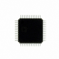
ADUC7060BSTZ32 Analog Devices Inc, ADUC7060BSTZ32 Datasheet - Page 44

ADUC7060BSTZ32
Manufacturer Part Number
ADUC7060BSTZ32
Description
DUAL 24-BIT AFE AND ARM 7 I.C
Manufacturer
Analog Devices Inc
Series
MicroConverter® ADuC7xxxr
Specifications of ADUC7060BSTZ32
Design Resources
4 mA-to-20 mA Loop-Powered Temperature Monitor Using ADuC7060/1 (CN0145) Low power, Long Range, ISM Wireless Measuring Node (CN0164)
Core Processor
ARM7
Core Size
16/32-Bit
Speed
10MHz
Connectivity
I²C, SPI, UART/USART
Peripherals
POR, PWM, Temp Sensor, WDT
Number Of I /o
14
Program Memory Size
32KB (16K x 16)
Program Memory Type
FLASH
Ram Size
4K x 8
Voltage - Supply (vcc/vdd)
2.375 V ~ 2.625 V
Data Converters
A/D 5x24b, 8x24b, D/A 1x14b
Oscillator Type
Internal
Operating Temperature
-40°C ~ 125°C
Package / Case
48-LQFP
Cpu Family
ADuC7xxx
Device Core
ARM7TDMI
Device Core Size
16/32Bit
Frequency (max)
10.24MHz
Interface Type
I2C/SPI/UART
Total Internal Ram Size
4KB
# I/os (max)
14
Number Of Timers - General Purpose
4
Operating Supply Voltage (typ)
2.5V
Operating Supply Voltage (max)
2.625V
Operating Supply Voltage (min)
2.375V
On-chip Adc
2(4-chx24-bit)
Instruction Set Architecture
RISC
Operating Temp Range
-40C to 125C
Operating Temperature Classification
Automotive
Mounting
Surface Mount
Pin Count
48
Package Type
LQFP
Package
48LQFP
Family Name
ADuC7xxx
Maximum Speed
10.24 MHz
Operating Supply Voltage
2.5 V
Data Bus Width
16|32 Bit
Number Of Programmable I/os
14
Number Of Timers
4
Lead Free Status / RoHS Status
Lead free / RoHS Compliant
Eeprom Size
-
Lead Free Status / Rohs Status
Compliant
Available stocks
Company
Part Number
Manufacturer
Quantity
Price
Company:
Part Number:
ADUC7060BSTZ32
Manufacturer:
CYPRESS
Quantity:
294
Company:
Part Number:
ADUC7060BSTZ32
Manufacturer:
ADI
Quantity:
315
Company:
Part Number:
ADUC7060BSTZ32
Manufacturer:
Analog Devices Inc
Quantity:
10 000
Part Number:
ADUC7060BSTZ32
Manufacturer:
ADI/亚德诺
Quantity:
20 000
Company:
Part Number:
ADUC7060BSTZ32-RL
Manufacturer:
Analog Devices Inc
Quantity:
10 000
ADuC7060/ADuC7061
Table 43. ADC0CON MMR Bit Designations
Bit
15
14:13
12
11
10
9:6
5:4
3:0
Name
ADC0EN
ADC0DIAG[1:0]
HIGHEXTREF0
AMP_CM
ADC0CODE
ADC0CH[3:0]
ADC0REF[1:0]
ADC0PGA[3:0].
Primary channel ADC enable.
Primary channel ADC output coding.
Primary channel ADC input select.
Primary channel ADC reference select.
Primary channel ADC gain select. Note, nominal primary ADC full-scale input voltage = (VREF/gain).
Description
This bit is set to 1 by user code to enable the primary ADC.
Clearing this bit to 0 powers down the primary ADC and resets the respective ADC ready bit in the ADCSTA MMR
to 0.
Diagnostic current source enable bits.
[00] = current sources off.
[01] = enables a 50 μA current source on the selected positive input (for example, ADC0).
[10] = enables a 50 μA current source on the selected negative input (for example, ADC1).
[11] = enables a 50 μA current source on both selected inputs (for example, ADC0 and ADC1).
This bit must be set high if the external reference for ADC0 exceeds 1.35 V. This results in the reference source
being divided by 2.
Clear this bit when using the internal reference or an external reference of less than 1.35 V.
This bit is set to 1 by user to set the PGA output common-mode voltage to AVDD/2.
This bit is cleared to 0 by user code to set the PGA output common-mode voltage to the PGA input common-
mode voltage level.
This bit is set to 1 by user code to configure primary ADC output coding as unipolar.
This bit is cleared to 0 by user code to configure primary ADC output coding as twos complement.
[0000] = ADC0/ADC1 (differential mode).
[0001] = ADC0/ADC5 (single-ended mode).
[0010] = ADC1/ADC5 (single-ended mode).
[0011] = VREF+, VREF−. Note: This is the reference selected by the ADC0REF bits.
[0100] = Not used. This bit combination is reserved for future functionality and should not be written.
[0101] = ADC2/ADC3 (differential mode).
[0110] = ADC2/ADC5 (single-ended mode).
[0111] = ADC3/ADC5 (single-ended mode).
[1000] = internal short to ADC0.
[1001] = internal short to ADC1.
[00] = internal reference selected. In ADC low power mode, the voltage reference selection is controlled by
ADCMDE[5].
[01] = external reference inputs (VREF+, VREF−) selected. Set the HIGHEXTREF0 bit if the reference voltage
exceeds 1.3 V.
[10] = auxiliary external reference inputs (ADC4/EXT_REF2IN+, ADC5/EXT_REF2IN−) selected. Set the
HIGHEXTREF0 bit if the reference voltage exceeds 1.3 V.
[11] = (AVDD, AGND) divide-by-two selected.
[0000] = ADC0 gain of 1. Buffer of negative input is bypassed.
[0001] = ADC0 gain of 2.
[0010] = ADC0 gain of 4 (default value). Enables the in-amp.
[0011] = ADC0 gain of 8.
[0100] = ADC0 gain of 16.
[0101] = ADC0 gain of 32.
[0110] = ADC0 gain of 64 (maximum PGA gain setting).
[0111] = ADC0 gain of 128 (extra gain implemented digitally).
[1000] = ADC0 gain of 256.
[1001] = ADC0 gain of 512.
[1XXX] = ADC0 gain is undefined.
Rev. B | Page 44 of 108


