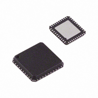
ADV7393BCPZ-REEL Analog Devices Inc, ADV7393BCPZ-REEL Datasheet - Page 20

ADV7393BCPZ-REEL
Manufacturer Part Number
ADV7393BCPZ-REEL
Description
IC,TV/VIDEO CIRCUIT,Video Encoder,LLCC,40PIN,PLASTIC
Manufacturer
Analog Devices Inc
Type
Video Encoderr
Datasheet
1.ADV7393BCPZ.pdf
(108 pages)
Specifications of ADV7393BCPZ-REEL
Design Resources
Reconstruction Video Filter Using ADA4430-1 Amplifier After ADV7393 Video Encoder (CN0101)
Applications
Set-Top Boxes, Video Players, Displays
Voltage - Supply, Analog
2.6 V ~ 3.46 V
Voltage - Supply, Digital
1.71 V ~ 1.89 V
Mounting Type
Surface Mount
Package / Case
40-LFCSP
Lead Free Status / RoHS Status
Lead free / RoHS Compliant
For Use With
ADV7393-DBRDZ - BOARD EVAL FOR ADV7393EVAL-ADV7393EBZ - BOARD EVAL FOR ADV7393 ENCODER
Lead Free Status / RoHS Status
Lead free / RoHS Compliant
- Current page: 20 of 108
- Download datasheet (2Mb)
ADV7390/ADV7391/ADV7392/ADV7393
ADV7390/
ADV7391
24
23
22, 21, 20
12
11
10
14
19
5, 28
1
17
16
15
18
6, 29
32
External Pad
1
2
ED = enhanced definition = 525p and 625p.
LSB = least significant bit. In the ADV7390/ADV7392, setting the LSB to 0 sets the I
ADV7391/ADV7393, setting the LSB to 0 sets the I
ADV7392/
ADV7393
30
29
28, 27, 26
14
13
12
20
25
6, 35
1
23
22
21
24
7, 36
40
External Pad
Pin No.
ADV7390
WLCSP
A1
C2
B1
F3
F2
E3
D3
C1
A3, D4
A5
E1
E2
F1
D1
C3, D5
D2
2
C address to 0x54. Setting it to 1 sets the I
Mnemonic
R
COMP
DAC 1
DAC 1, DAC 2,
DAC 3
SCL
SDA
ALSB
RESET
V
V
V
PV
EXT_LF
PGND
AGND
DGND
GND_IO
EPAD
SET
AA
DD
DD_IO
DD
Rev. B | Page 20 of 108
2
C address to 0xD4. Setting it to 1 sets the I
Input/
Output
I
O
O
O
I
I/O
I
I
P
P
P
P
I
G
G
G
G
G
2
C address to 0x56.
Description
Controls the amplitudes of the DAC 1, DAC 2, and DAC 3
outputs. For full-drive operation (for example, into a 37.5 Ω
load), a 510 Ω resistor must be connected from R
AGND. For low-drive operation (for example, into a 300 Ω
load), a 4.12 kΩ resistor must be connected from R
AGND.
Compensation Pin. Connect a 2.2 nF capacitor from COMP
to V
DAC Output. Full-drive and low-drive capable DAC
DAC Outputs. Full-drive and low-drive capable DACs.
I
I
ALSB sets up the LSB
Resets the on-chip timing generator and sets the ADV739x
into its default mode.
Analog Power Supply (2.7 V or 3.3 V).
Digital Power Supply (1.8 V). For dual-supply
configurations, V
supplies through a ferrite bead or suitable filtering.
Input/Output Digital Power Supply (1.8 V or 3.3 V).
PLL Power Supply (1.8 V). For dual-supply configurations,
PV
ferrite bead or suitable filtering.
External Loop Filter for the Internal PLL.
PLL Ground Pin.
Analog Ground Pin.
Digital Ground Pin.
Input/Output Supply Ground Pin.
Connect to analog ground (AGND).
2
2
C Clock Input.
C Data Input/Output.
DD
AA
can be connected to other 1.8 V supplies through a
.
DD
can be connected to other 1.8 V
2
of the MPU I
2
C address to 0xD6. In the
2
C address.
SET
SET
to
to
Related parts for ADV7393BCPZ-REEL
Image
Part Number
Description
Manufacturer
Datasheet
Request
R

Part Number:
Description:
EVALUATION BOARD I.C.
Manufacturer:
Analog Devices Inc
Datasheet:

Part Number:
Description:
±1.7g Dual-Axis IMEMS Accelerometer Evaluation Board
Manufacturer:
Analog Devices Inc
Datasheet:

Part Number:
Description:
Inertial Sensor Evaluation System
Manufacturer:
Analog Devices Inc
Datasheet:

Part Number:
Description:
Manufacturer:
Analog Devices Inc
Datasheet:

Part Number:
Description:
Manufacturer:
Analog Devices Inc
Datasheet:

Part Number:
Description:
Manufacturer:
Analog Devices Inc
Datasheet:

Part Number:
Description:
Manufacturer:
Analog Devices Inc
Datasheet:

Part Number:
Description:
Manufacturer:
Analog Devices Inc
Datasheet:

Part Number:
Description:
Manufacturer:
Analog Devices Inc
Datasheet:

Part Number:
Description:
Manufacturer:
Analog Devices Inc
Datasheet:

Part Number:
Description:
Manufacturer:
Analog Devices Inc
Datasheet:

Part Number:
Description:
Manufacturer:
Analog Devices Inc
Datasheet:

Part Number:
Description:
Manufacturer:
Analog Devices Inc
Datasheet:


