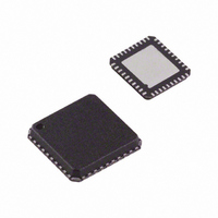
ADV7393BCPZ-REEL Analog Devices Inc, ADV7393BCPZ-REEL Datasheet - Page 65

ADV7393BCPZ-REEL
Manufacturer Part Number
ADV7393BCPZ-REEL
Description
IC,TV/VIDEO CIRCUIT,Video Encoder,LLCC,40PIN,PLASTIC
Manufacturer
Analog Devices Inc
Type
Video Encoderr
Datasheet
1.ADV7393BCPZ.pdf
(108 pages)
Specifications of ADV7393BCPZ-REEL
Design Resources
Reconstruction Video Filter Using ADA4430-1 Amplifier After ADV7393 Video Encoder (CN0101)
Applications
Set-Top Boxes, Video Players, Displays
Voltage - Supply, Analog
2.6 V ~ 3.46 V
Voltage - Supply, Digital
1.71 V ~ 1.89 V
Mounting Type
Surface Mount
Package / Case
40-LFCSP
Lead Free Status / RoHS Status
Lead free / RoHS Compliant
For Use With
ADV7393-DBRDZ - BOARD EVAL FOR ADV7393EVAL-ADV7393EBZ - BOARD EVAL FOR ADV7393 ENCODER
Lead Free Status / RoHS Status
Lead free / RoHS Compliant
EXTERNAL HORIZONTAL AND VERTICAL SYNCHRONIZATION CONTROL
For timing synchronization purposes, the ADV739x is able to accept either EAV/SAV time codes embedded in the input pixel data or
external synchronization signals provided on the HSYNC and VSYNC pins (see
signals on the
Table 54. Timing Synchronization Signal Input Options
Signal
SD HSYNC In
SD VSYNC/FIELD In
ED/HD HSYNC In
ED/HD VSYNC/FIELD In
1
Table 55. Timing Synchronization Signal Output Options
Signal
SD HSYNC Out
SD VSYNC/FIELD Out
ED/HD HSYNC Out
ED/HD VSYNC/FIELD Out
1
2
Table 56. HSYNC Output Control
ED/HD Input Sync Format
(Subaddress 0x30,
Bit 2)
X
X
0
1
X
1
2
Table 57. VSYNC Output Control
ED/HD Input
Sync Format
(Subaddress
0x30, Bit 2)
x
x
0
1
1
SD and ED/HD timing synchronization outputs must also be disabled (Subaddress 0x02[7:6] = 00).
ED/HD timing synchronization outputs must also be disabled (Subaddress 0x02, Bit 7 = 0).
ED/HD timing synchronization inputs must also be disabled; that is, embedded EAV/SAV timing codes must be enabled (Subaddress 0x30, Bit 2 = 1).
In all ED/HD standards where there is an HSYNC output, the start of the HSYNC pulse is aligned with the falling edge of the embedded HSYNC in the output video.
X = don’t care.
HSYNC and VSYNC pins (see
ED/HD VSYNC
Control
(Subaddress
0x34, Bit 2)
x
x
0
0
0
Pin
HSYNC
VSYNC
HSYNC
VSYNC
Pin
HSYNC
VSYNC
HSYNC
VSYNC
ED/HD HSYNC Control
(Subaddress 0x34,
Bit 1)
X
X
0
0
1
1, 2
, 1 2
ED/HD Sync
Output Enable
(Subaddress
0x02, Bit 7)
0
0
1
1
1
Table 55
Condition
Condition
ED/HD Sync
Output Enable
(Subaddress 0x02,
Bit 7)
0
0
1
1
1
SD slave timing (Mode 1, Mode 2, or Mode 3) selected (Subaddress 0x8A[2:0])
SD slave timing (Mode 1, Mode 2, or Mode 3) selected (Subaddress 0x8A[2:0])
ED/HD timing synchronization inputs enabled (Subaddress 0x30, Bit 2 = 0)
ED/HD timing synchronization inputs enabled (Subaddress 0x30, Bit 2 = 0)
SD timing synchronization outputs enabled (Subaddress 0x02, Bit 6 = 1)
SD timing synchronization outputs enabled (Subaddress 0x02, Bit 6 = 1)
ED/HD timing synchronization outputs enabled (Subaddress 0x02, Bit 7 = 1)
ED/HD timing synchronization outputs enabled (Subaddress 0x02, Bit 7 = 1)
to
SD Sync
Output Enable
(Subaddress
0x02, Bit 6)
0
1
x
x
x
Table 57
Rev. B | Page 65 of 108
).
SD Sync
Output Enable
(Subaddress 0x02,
Bit 6)
0
1
X
X
X
Video Standard
x
Interlaced
x
All HD interlaced
standards
All ED/HD
progressive
standards
ADV7390/ADV7391/ADV7392/ADV7393
Table 54
). It is also possible to output synchronization
Signal on HSYNC Pin
Tristate
Pipelined SD HSYNC
Pipelined ED/HD HSYNC
Pipelined ED/HD HSYNC
based on AV Code H bit
Pipelined ED/HD HSYNC
based on horizontal
counter
Signal on VSYNC Pin
Tristate
Pipelined SD VSYNC/field
Pipelined ED/HD VSYNC
or field signal
Pipelined field signal
based on AV Code F bit
Pipelined VSYNC based
on AV Code V bit
1
1
Duration
N/A
See the
section.
As per HSYNC
timing.
Same as line
blanking interval.
Same as embedded
HSYNC.
Duration
See the
section.
As per VSYNC or
field signal timing.
Field.
Vertical blanking
interval.
N/A
2
2
1
1
SD Timing
SD Timing


