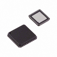
ADV7393BCPZ-REEL Analog Devices Inc, ADV7393BCPZ-REEL Datasheet - Page 71

ADV7393BCPZ-REEL
Manufacturer Part Number
ADV7393BCPZ-REEL
Description
IC,TV/VIDEO CIRCUIT,Video Encoder,LLCC,40PIN,PLASTIC
Manufacturer
Analog Devices Inc
Type
Video Encoderr
Datasheet
1.ADV7393BCPZ.pdf
(108 pages)
Specifications of ADV7393BCPZ-REEL
Design Resources
Reconstruction Video Filter Using ADA4430-1 Amplifier After ADV7393 Video Encoder (CN0101)
Applications
Set-Top Boxes, Video Players, Displays
Voltage - Supply, Analog
2.6 V ~ 3.46 V
Voltage - Supply, Digital
1.71 V ~ 1.89 V
Mounting Type
Surface Mount
Package / Case
40-LFCSP
Lead Free Status / RoHS Status
Lead free / RoHS Compliant
For Use With
ADV7393-DBRDZ - BOARD EVAL FOR ADV7393EVAL-ADV7393EBZ - BOARD EVAL FOR ADV7393 ENCODER
Lead Free Status / RoHS Status
Lead free / RoHS Compliant
Power Supply Decoupling
It is recommended that each power supply pin be decoupled
with 10 nF and 0.1 μF ceramic capacitors. The V
V
ground. The decoupling capacitors should be placed as close as
possible to the ADV739x with the capacitor leads kept as short
as possible to minimize lead inductance.
A 1 μF tantalum capacitor is recommended across the V
supply in addition to the 10 nF and 0.1 μF ceramic capacitors.
Power Supply Sequencing
The ADV739x is robust to all power supply sequencing combin-
ations. Any sequence can be used. However, all power supplies
should settle to their nominal voltages within one second.
Digital Signal Interconnect
The digital signal traces should be isolated as much as possible
from the analog outputs and other analog circuitry. Digital
signal traces should not overlay the V
Due to the high clock rates used, avoid long clock traces to the
ADV739x to minimize noise pickup.
Any pull-up termination resistors for the digital inputs should
be connected to the V
Analog Signal Interconnect
DAC output traces should be treated as transmission lines with
appropriate measures taken to ensure optimal performance (for
example, impedance matched traces). The DAC output traces
should be kept as short as possible. The termination resistors on
the DAC output traces should be placed as close as possible to,
and on the same side of the PCB as, the ADV739x.
To avoid crosstalk between the DAC outputs, it is recommended
that as much space as possible be left between the traces
connected to the DAC output pins. Adding ground traces
between the DAC output traces is also recommended.
DD_IO
, and both V
DD
pins should be individually decoupled to
DD_IO
power supply.
AA
or PV
DD
AA
power plane.
, PV
DD
AA
,
Rev. B | Page 71 of 108
ADDITIONAL LAYOUT CONSIDERATIONS FOR THE
WLCSP PACKAGE
Due to the high pad density and 0.5 mm pitch of the WLCSP, it
is not recommended that connections to inner bumps be routed
on the top PCB layer only.
The traces (track and space) must fit within the limits of the
solder mask openings. Routing all traces on the top surface
layer of the board, while possible, is usually not a feasible
solution due to the limitations of the geometries imposed by
the board fabrication technology. Given a pitch of 0.5 mm with
a typical solder mask opening diameter of 0.35 mm, there is only
a 0.15 mm distance between the solder mask openings.
An alternative to routing on the top surface is to route out on
buried layers. To achieve this, the pads are connected to the
lower layers using microvias. See the AN-617 Application Note,
MicroCSP Wafer Level Chip Scale Package for additional details
about the board layout for the WLCSP package.
ADV7390/ADV7391/ADV7392/ADV7393


