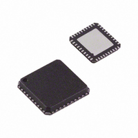
ADV7393BCPZ-REEL Analog Devices Inc, ADV7393BCPZ-REEL Datasheet - Page 61

ADV7393BCPZ-REEL
Manufacturer Part Number
ADV7393BCPZ-REEL
Description
IC,TV/VIDEO CIRCUIT,Video Encoder,LLCC,40PIN,PLASTIC
Manufacturer
Analog Devices Inc
Type
Video Encoderr
Datasheet
1.ADV7393BCPZ.pdf
(108 pages)
Specifications of ADV7393BCPZ-REEL
Design Resources
Reconstruction Video Filter Using ADA4430-1 Amplifier After ADV7393 Video Encoder (CN0101)
Applications
Set-Top Boxes, Video Players, Displays
Voltage - Supply, Analog
2.6 V ~ 3.46 V
Voltage - Supply, Digital
1.71 V ~ 1.89 V
Mounting Type
Surface Mount
Package / Case
40-LFCSP
Lead Free Status / RoHS Status
Lead free / RoHS Compliant
For Use With
ADV7393-DBRDZ - BOARD EVAL FOR ADV7393EVAL-ADV7393EBZ - BOARD EVAL FOR ADV7393 ENCODER
Lead Free Status / RoHS Status
Lead free / RoHS Compliant
- Current page: 61 of 108
- Download datasheet (2Mb)
ED/HD SHARPNESS FILTER AND ADAPTIVE FILTER
APPLICATION EXAMPLES
Sharpness Filter Application
The ED/HD sharpness filter can be used to enhance or
attenuate the Y video output signal. The register settings in
Table 52 are used to achieve the results shown in Figure 77.
Input data is generated by an external signal source.
Table 52. ED/HD Sharpness Control Settings for Figure 77
Subaddress
0x00
0x01
0x02
0x30
0x31
0x40
0x40
0x40
0x40
0x40
0x40
1
See Figure 77.
SIGNAL
INPUT
STEP
Block
R2
R4
1
1.5
1.4
1.3
1.2
1.1
1.0
0.9
0.8
0.7
0.6
0.5
CH1
REF A
Register Setting
0xFC
0x10
0x20
0x00
0x81
0x00
0x08
0x04
0x40
0x80
0x22
500mV
Figure 77. ED/HD Sharpness Filter Control with Different Gain Settings for ED/HD Sharpness Filter Gain Values
FILTER A RESPONSE (Gain Ka)
FREQUENCY (MHz)
500mV 4.00µs
SHARPNESS AND ADAPTIVE FILTER CONTROL BLOCK
1
M 4.00µs
Figure 76. ED/HD Sharpness and Adaptive Filter Control
9.99978ms
Reference
a
b
c
d
e
f
1.5
1.4
1.3
1.2
1.1
1.0
0.9
0.8
0.7
0.6
0.5
1
ALL FIELDS
Rev. B | Page 61 of 108
FILTER B RESPONSE (Gain Kb)
CH1
FREQUENCY (MHz)
b
a
c
R1
R2
1
Adaptive Filter Control Application
The register settings in Table 53 are used to obtain the results
shown in Figure 79, that is, to remove the ringing on the input
Y signal, as shown in Figure 78. Input data is generated by an
external signal source.
Table 53. Register Settings for Figure 79
Subaddress
0x00
0x01
0x02
0x30
0x31
0x35
0x40
0x58
0x59
0x5A
0x5B
0x5C
0x5D
CH1
REF A
ADV7390/ADV7391/ADV7392/ADV7393
500mV
500mV 4.00µs
1.6
1.5
1.4
1.3
1.2
1.1
1.0
FREQUENCY RESPONSE IN SHARPNESS
0
FILTER MODE WITH Ka = 3 AND Kb = 7
1
M 4.00µs
2
Register Setting
0xFC
0x38
0x20
0x00
0x81
0x80
0x00
0xAC
0x9A
0x88
0x28
0x3F
0x64
9.99978ms
FREQUENCY (MHz)
4
6
ALL FIELDS
8
10
CH1
d
e
f
12
Related parts for ADV7393BCPZ-REEL
Image
Part Number
Description
Manufacturer
Datasheet
Request
R

Part Number:
Description:
EVALUATION BOARD I.C.
Manufacturer:
Analog Devices Inc
Datasheet:

Part Number:
Description:
±1.7g Dual-Axis IMEMS Accelerometer Evaluation Board
Manufacturer:
Analog Devices Inc
Datasheet:

Part Number:
Description:
Inertial Sensor Evaluation System
Manufacturer:
Analog Devices Inc
Datasheet:

Part Number:
Description:
Manufacturer:
Analog Devices Inc
Datasheet:

Part Number:
Description:
Manufacturer:
Analog Devices Inc
Datasheet:

Part Number:
Description:
Manufacturer:
Analog Devices Inc
Datasheet:

Part Number:
Description:
Manufacturer:
Analog Devices Inc
Datasheet:

Part Number:
Description:
Manufacturer:
Analog Devices Inc
Datasheet:

Part Number:
Description:
Manufacturer:
Analog Devices Inc
Datasheet:

Part Number:
Description:
Manufacturer:
Analog Devices Inc
Datasheet:

Part Number:
Description:
Manufacturer:
Analog Devices Inc
Datasheet:

Part Number:
Description:
Manufacturer:
Analog Devices Inc
Datasheet:

Part Number:
Description:
Manufacturer:
Analog Devices Inc
Datasheet:


