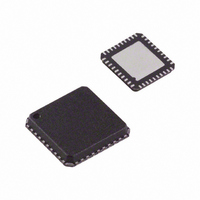
ADV7393BCPZ-REEL Analog Devices Inc, ADV7393BCPZ-REEL Datasheet - Page 32

ADV7393BCPZ-REEL
Manufacturer Part Number
ADV7393BCPZ-REEL
Description
IC,TV/VIDEO CIRCUIT,Video Encoder,LLCC,40PIN,PLASTIC
Manufacturer
Analog Devices Inc
Type
Video Encoderr
Datasheet
1.ADV7393BCPZ.pdf
(108 pages)
Specifications of ADV7393BCPZ-REEL
Design Resources
Reconstruction Video Filter Using ADA4430-1 Amplifier After ADV7393 Video Encoder (CN0101)
Applications
Set-Top Boxes, Video Players, Displays
Voltage - Supply, Analog
2.6 V ~ 3.46 V
Voltage - Supply, Digital
1.71 V ~ 1.89 V
Mounting Type
Surface Mount
Package / Case
40-LFCSP
Lead Free Status / RoHS Status
Lead free / RoHS Compliant
For Use With
ADV7393-DBRDZ - BOARD EVAL FOR ADV7393EVAL-ADV7393EBZ - BOARD EVAL FOR ADV7393 ENCODER
Lead Free Status / RoHS Status
Lead free / RoHS Compliant
- Current page: 32 of 108
- Download datasheet (2Mb)
ADV7390/ADV7391/ADV7392/ADV7393
Table 21. Register 0x31 to Register 0x33
SR7 to
SR0
0x31
0x32
0x33
1
Available on the ADV7392/ADV7393 (40-pin devices) only.
Register
ED/HD Mode
Register 2
ED/HD Mode
Register 3
ED/HD Mode
Register 4
Bit Description
ED/HD pixel data valid
HD oversample rate select
ED/HD test pattern enable
ED/HD test pattern hatch/field
ED/HD vertical blanking interval (VBI)
open
ED/HD undershoot limiter
ED/HD sharpness filter
ED/HD Y delay with respect to the
falling edge of HSYNC
ED/HD color delay with respect to the
falling edge of HSYNC
ED/HD CGMS enable
ED/HD CGMS CRC enable
ED/HD Cr/Cb sequence
Reserved
ED/HD input form
Sinc compensation filter on DAC 1, DAC
2, DAC 3
Reserved
ED/HD chroma SSAF filter
Reserved
ED/HD double buffering
at
Rev. B | Page 32 of 108
1
1
0
1
7
0
0
6
0
0
1
1
0
1
1
5
0
1
0
1
0
0
0
0
1
0
1
Bit Number
4
0
1
0
0
1
1
0
0
3
1
0
1
0
1
0
0
1
0
2
0
1
0
0
0
0
1
0
1
1
0
1
0
0
1
1
0
0
0
0
1
0
1
0
1
0
0
1
Register Setting
Pixel data valid off.
Pixel data valid on.
4×.
2×.
HD test pattern off.
HD test pattern on.
Hatch.
Field/frame.
Disabled.
Enabled.
Disabled.
−11 IRE.
−6 IRE.
−1.5 IRE.
Disabled.
Enabled.
0 clock cycles.
One clock cycle.
Two clock cycles.
Three clock cycles.
Four clock cycles.
0 clock cycles.
One clock cycle.
Two clock cycles.
Three clock cycles.
Four clock cycles.
Disabled.
Enabled.
Disabled.
Enabled.
Cb after falling edge of HSYNC.
Cr after falling edge of HSYNC.
0 must be written to this bit.
8-bit input.
10-bit input
Disabled.
Enabled.
0 must be written to this bit.
Disabled.
Enabled.
1 must be written to this bit.
Disabled.
Enabled.
1
.
Reset
Value
0x00
0x00
0x68
Related parts for ADV7393BCPZ-REEL
Image
Part Number
Description
Manufacturer
Datasheet
Request
R

Part Number:
Description:
EVALUATION BOARD I.C.
Manufacturer:
Analog Devices Inc
Datasheet:

Part Number:
Description:
±1.7g Dual-Axis IMEMS Accelerometer Evaluation Board
Manufacturer:
Analog Devices Inc
Datasheet:

Part Number:
Description:
Inertial Sensor Evaluation System
Manufacturer:
Analog Devices Inc
Datasheet:

Part Number:
Description:
Manufacturer:
Analog Devices Inc
Datasheet:

Part Number:
Description:
Manufacturer:
Analog Devices Inc
Datasheet:

Part Number:
Description:
Manufacturer:
Analog Devices Inc
Datasheet:

Part Number:
Description:
Manufacturer:
Analog Devices Inc
Datasheet:

Part Number:
Description:
Manufacturer:
Analog Devices Inc
Datasheet:

Part Number:
Description:
Manufacturer:
Analog Devices Inc
Datasheet:

Part Number:
Description:
Manufacturer:
Analog Devices Inc
Datasheet:

Part Number:
Description:
Manufacturer:
Analog Devices Inc
Datasheet:

Part Number:
Description:
Manufacturer:
Analog Devices Inc
Datasheet:

Part Number:
Description:
Manufacturer:
Analog Devices Inc
Datasheet:


