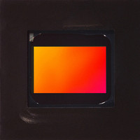
MT9V022IA7ATM Aptina LLC, MT9V022IA7ATM Datasheet - Page 30

MT9V022IA7ATM
Manufacturer Part Number
MT9V022IA7ATM
Description
SENSOR IMAGE VGA MONO 52IBGA
Manufacturer
Aptina LLC
Type
CMOS Imagingr
Series
DigitalClarity®r
Specifications of MT9V022IA7ATM
Pixel Size
6µm x 6µm
Active Pixel Array
752H x 480V
Frames Per Second
60
Voltage - Supply
3.3V
Package / Case
52-IBGA
Sensor Image Color Type
Monochrome
Sensor Image Size Range
250,920 to 480,000Pixels
Sensor Image Size
752x480Pixels
Operating Supply Voltage (min)
3V
Operating Supply Voltage (typ)
3.3V
Operating Supply Voltage (max)
3.6V
Operating Temp Range
-40C to 85C
Package Type
IBGA
Operating Temperature Classification
Industrial
Mounting
Surface Mount
Pin Count
52
Lead Free Status / RoHS Status
Lead free / RoHS Compliant
Other names
557-1205
Available stocks
Company
Part Number
Manufacturer
Quantity
Price
Black Level Calibration
Figure 26:
PDF: 3295348826/Source:7478516499
MT9V022_DS - Rev.H 6/10 EN
Black Level Calibration Flow Chart
Voltage (R0x48 or
Offset Correction
Registers 0x99
Figure 25, respectively.
Digital gains of registers 0x80
supports a digital gain of 0.25-3.75X.
Black level calibration is controlled by:
• R0x4C
• R0x42
• R0x46–R0x48
The MT9V022 has automatic black level calibration on-chip, and if enabled, its result
may be used in the offset correction shown in Figure 26.
The automatic black level calibration measures the average value of pixels from 2 dark
rows (1 dark row if row bin 4 is enabled) of the chip. (The pixels are averaged as if they
were light-sensitive and passed through the appropriate gain.)
This row average is then digitally low-pass filtered over many frames (R0x47, bits 7:5) to
remove temporal noise and random instabilities associated with this measurement.
Then, the new filtered average is compared to a minimum acceptable level, low
threshold, and a maximum acceptable level, high threshold.
If the average is lower than the minimum acceptable level, the offset correction voltage
is increased by a programmable offset LSB in R0x4C. (Default step size is 2 LSB Offset = 1
ADC LSB at analog gain = 1X.)
If it is above the maximum level, the offset correction voltage is decreased by 2 LSB
(default).
To avoid oscillation of the black level from below to above, the region the thresholds
should be programmed so the difference is at least two times the offset DAC step size.
result of BLC)
The formula for digital gain setting is:
(reset minus signal)
Pixel Output
Digital Gain = Bits[3:0] x 0.25
–
0x9E and 0x9F
S
C1
–
–
30
0x98 apply to their corresponding tiles. The MT9V022
0xA4 represent the coordinates X
C2
MT9V022: 1/3-Inch Wide-VGA Digital Image Sensor
Gain Selection
result of AGC)
(R0x35 or
Aptina reserves the right to change products or specifications without notice.
10 (12) bit ADC
(R0x2C)
©2005 Aptina Imaging Corporation. All rights reserved.
0/5
V
REF
-X
Feature Description
5/5
and Y
0/5
ADC Data
-Y
(9:0)
(EQ 8)
5/5
in


