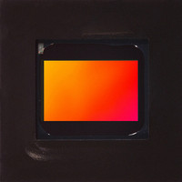
MT9V022IA7ATM Aptina LLC, MT9V022IA7ATM Datasheet - Page 41

MT9V022IA7ATM
Manufacturer Part Number
MT9V022IA7ATM
Description
SENSOR IMAGE VGA MONO 52IBGA
Manufacturer
Aptina LLC
Type
CMOS Imagingr
Series
DigitalClarity®r
Specifications of MT9V022IA7ATM
Pixel Size
6µm x 6µm
Active Pixel Array
752H x 480V
Frames Per Second
60
Voltage - Supply
3.3V
Package / Case
52-IBGA
Sensor Image Color Type
Monochrome
Sensor Image Size Range
250,920 to 480,000Pixels
Sensor Image Size
752x480Pixels
Operating Supply Voltage (min)
3V
Operating Supply Voltage (typ)
3.3V
Operating Supply Voltage (max)
3.6V
Operating Temp Range
-40C to 85C
Package Type
IBGA
Operating Temperature Classification
Industrial
Mounting
Surface Mount
Pin Count
52
Lead Free Status / RoHS Status
Lead free / RoHS Compliant
Other names
557-1205
Available stocks
Company
Part Number
Manufacturer
Quantity
Price
Table 11:
Table 12:
Propagation Delays for PIXCLK and Data Out Signals
PDF: 3295348826/Source:7478516499
MT9V022_DS - Rev.H 6/10 EN
Symbol
SYSCLK
t
t
t
t
t
t
t
t
R
F
PLH
PD
SD
HD
PFLR
PFLF
P
Symbol
V
I
T
SUPPLY
V
SUPPLY
I
GND
V
STG
OUT
IN
1
PIXCLK to FRAME_VALID propagation delay
Input clock frequency
Clock duty cycle
Input clock rise time
Input clock fall time
SYSCLK to PIXCLK propagation delay
PIXCLK to valid D
Data setup time
Data hold time
PIXCLK to LINE_VALID propagation delay
Absolute Maximum Ratings
AC Electrical Characteristics
V
PWR
Caution
= 3.3V ±0.3V; T
Notes:
Notes:
Power supply voltage (all supplies)
Total power supply current
Total ground current
DC input voltage
DC output voltage
Storage temperature
OUT
Stresses greater than those listed may cause permanent damage to the device.
The pixel clock is inverted and delayed relative to the master clock. The relative delay
from the master clock (SYSCLK) rising edge to both the pixel clock (PIXCLK) falling edge
and the data output transition is typically 7ns. Note that the falling edge of the pixel
clock occurs at approximately the same time as the data output transitions. See Table 12
for data setup and hold times.
1. This is a stress rating only, and functional operation of the device at these or any other conditions above
1. The frequency range specified applies only to the parallel output mode of operation.
(9:0) propagation delay
Definition
those indicated in the operational sections of this specification is not implied.
Exposure to absolute maximum rating conditions for extended periods may affect
reliability.
A
= Ambient = 25
Parameter
°
C; Output Load = 10pF
41
C
C
C
C
LOAD
LOAD
LOAD
LOAD
Condition
Note 1
MT9V022: 1/3-Inch Wide-VGA Digital Image Sensor
= 10pF
= 10pF
= 10pF
= 10pF
Minimum
–0.3
–0.3
–0.3
–40
–
–
Minimum
13.0
45.0
–2
14
14
–2
–2
1
1
3
Maximum
V
V
Aptina reserves the right to change products or specifications without notice.
DD
DD
+125
200
200
4.5
+ 0.3
+ 0.3
Typical
26.6
50.0
16
16
2
2
7
0
0
0
©2005 Aptina Imaging Corporation. All rights reserved.
Electrical Specifications
Unit
mA
mA
°C
V
V
V
Maximum
27.0
55.0
11
5
5
2
–
–
2
2
MHz
Unit
ns
ns
ns
ns
ns
ns
ns
%


