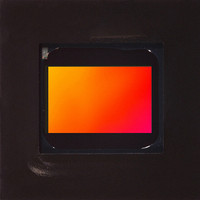
MT9V022IA7ATM Aptina LLC, MT9V022IA7ATM Datasheet - Page 31

MT9V022IA7ATM
Manufacturer Part Number
MT9V022IA7ATM
Description
SENSOR IMAGE VGA MONO 52IBGA
Manufacturer
Aptina LLC
Type
CMOS Imagingr
Series
DigitalClarity®r
Specifications of MT9V022IA7ATM
Pixel Size
6µm x 6µm
Active Pixel Array
752H x 480V
Frames Per Second
60
Voltage - Supply
3.3V
Package / Case
52-IBGA
Sensor Image Color Type
Monochrome
Sensor Image Size Range
250,920 to 480,000Pixels
Sensor Image Size
752x480Pixels
Operating Supply Voltage (min)
3V
Operating Supply Voltage (typ)
3.3V
Operating Supply Voltage (max)
3.6V
Operating Temp Range
-40C to 85C
Package Type
IBGA
Operating Temperature Classification
Industrial
Mounting
Surface Mount
Pin Count
52
Lead Free Status / RoHS Status
Lead free / RoHS Compliant
Other names
557-1205
Available stocks
Company
Part Number
Manufacturer
Quantity
Price
Row-wise Noise Correction
PDF: 3295348826/Source:7478516499
MT9V022_DS - Rev.H 6/10 EN
Offset Correction Voltage = (8-bit signed two’s complement calibration value,-127 to 127) × 0.5mV
ADC input voltage = (Pixel Output Voltage + Offset Correction Voltage) × Analog Gain
777 < (R0x73, bits 9:0) + number of dark pixels programmed in R0x70, bits 3:0 -1
Pixel value = ADC value - dark column average + row noise constant
In normal operation, the black level calibration value/offset correction value is calcu-
lated at the beginning of each frame and can be read through the two-wire serial inter-
face from R0x48. This register is an 8-bit signed two’s complement value.
However, if R0x47, bit 0 is set to “1,” the calibration value in R0x48 may be manually set
to override the automatic black level calculation result. This feature can be used in
conjunction with the “show dark rows” feature (R0x0D, bit 6) if using an external black
level calibration circuit.
The offset correction voltage is generated according to the following formulas:
Row-wise noise correction is controlled by the following registers:
• R0x70 Row Noise Control
• R0x72 Row Noise Constant
• R0x73 Dark Column Start
When the row-wise noise cancellation algorithm is enabled, the average value of the
dark columns read out is used as a correction for the whole row. The row-wise correction
is in addition to the general black level correction applied to the whole sensor frame and
cannot be used to replace the latter. The dark average is subtracted from each pixel
belonging to the same row, and then a positive constant is added (R0x72, bits 7:0). This
constant should be set to the dark level targeted by the black level algorithm plus the
noise expected on the measurements of the averaged values from dark columns; it is
meant to prevent clipping from negative noise fluctuations.
On a per-row basis, the dark column average is calculated from a programmable
number of dark columns (pixels) values (R0x70, bits 3:0). The default is 10 dark columns.
Of these, the maximum and minimum values are removed and then the average is calcu-
lated. If R0x70, bits 3:0 are set to “0” (2 pixels), it is essentially equivalent to disabling the
dark average calculation since the average is equal to “0” after the maximum and
minimum values are removed.
R0x73 is used to indicate the starting column address of dark pixels which row-noise
correction algorithm uses for calculation. In the MT9V022, dark columns which may be
used are 759–776. R0x73 is used to select the starting column for the calculation.
One additional note in setting the row-noise correction register:
This is to ensure the column pointer does not go beyond the limit the MT9V022 can
support.
31
MT9V022: 1/3-Inch Wide-VGA Digital Image Sensor
Aptina reserves the right to change products or specifications without notice.
©2005 Aptina Imaging Corporation. All rights reserved.
Feature Description
(EQ 10)
(EQ 11)
(EQ 12)
(EQ 9)


