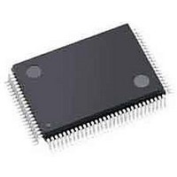
ISPPAC-CLK5620V-01TN100I Lattice, ISPPAC-CLK5620V-01TN100I Datasheet - Page 16

ISPPAC-CLK5620V-01TN100I
Manufacturer Part Number
ISPPAC-CLK5620V-01TN100I
Description
Clock Drivers & Distribution PROGRAMMABLE ZERO DELAY CL GEN
Manufacturer
Lattice
Type
Zero Delay Programmable PLL Clock Generatorr
Datasheet
1.ISPPAC-CLK5620V-01TN100C.pdf
(49 pages)
Specifications of ISPPAC-CLK5620V-01TN100I
Max Input Freq
320 MHz
Minimum Operating Temperature
- 40 C
Mounting Style
SMD/SMT
Supply Voltage (max)
3.6 V
Supply Voltage (min)
3 V
Maximum Operating Temperature
+ 85 C
Package / Case
TQFP-100
Lead Free Status / RoHS Status
Lead free / RoHS Compliant
Available stocks
Company
Part Number
Manufacturer
Quantity
Price
Company:
Part Number:
ISPPAC-CLK5620V-01TN100I
Manufacturer:
Lattice Semiconductor Corporation
Quantity:
10 000
Lattice Semiconductor
phase-lock mode, the LOCK signal is asserted if the phases of the reference and feedback signals match, whereas
in frequency-lock mode the LOCK signal is asserted when the frequencies of the feedback and reference signals
match. The option of which mode to use is programmable and may be set using PAC-Designer software (available
from the Lattice web site at www.latticesemi.com).
In phase-lock mode the lock detector asserts the LOCK signal as soon as a lock condition is determined. In fre-
quency-lock mode, however, the PLL must be in a locked condition for a set number of phase detector cycles
before the LOCK signal will be asserted. The number of cycles required before asserting the LOCK signal in fre-
quency-lock mode can be set from 16 through 256.
When the lock condition is lost the LOCK signal will be de-asserted immediately in both phase-lock and frequency-
lock detection modes. In frequency-lock mode, however, if the input reference signal is stopped, the LOCK output
may continue to be asserted. In phase-lock mode, a loss of the input reference signal will always result in de-asser-
tion of the LOCK output.
Loop Filter
A simplified schematic for the ispClock5600 loop filter is shown in Figure 11. The filter’s capacitors are fixed, and
the response is controlled by setting the value of the phase-detector’s output current source’s and the value of the
variable resistor. The phase detector output current has 14 possible settings, ranging from 3µA to 55µA, while the
resistor may be set to any one of six values ranging from 2.3K to 9.3K. This provides a total of 84 unique I-R com-
binations which may be selected.
Figure 11. ispClock5600 Loop Filter (Simplified)
Because the selection of an optimal PLL loop filter can be a daunting task, PAC-Designer offers a set of default fil-
ter settings which will provide acceptable performance for most applications. The primary criterion for selecting one
of these settings is the total division factor used in the feedback path. This factor is the ratio between the VCO out-
put frequency and the feedback V-divider output frequency which is the product of the N-divider and V
divider (N x V
able V x V
used to optimize overall jitter performance including phase jitter.
feedback
feedback
values. Table 2 should be used to minimize cycle to cycle and period jitter while Table 3 should be
). Table 2 and Table 3 list the default loop filter settings that correspond to all possible allow-
M-divider
N-divider
From
From
Phase Detector
I
I
16
C
1
ispClock5600 Family Data Sheet
R
C
2
To VCO
feedback
-


