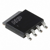
PSMN4R0-40YS,115 NXP Semiconductors, PSMN4R0-40YS,115 Datasheet - Page 6

PSMN4R0-40YS,115
Manufacturer Part Number
PSMN4R0-40YS,115
Description
MOSFET N-CH 40V 100A LFPAK
Manufacturer
NXP Semiconductors
Datasheet
1.PSMN4R0-40YS115.pdf
(15 pages)
Specifications of PSMN4R0-40YS,115
Package / Case
LFPak-4
Fet Type
MOSFET N-Channel, Metal Oxide
Fet Feature
Standard
Rds On (max) @ Id, Vgs
4.2 mOhm @ 15A, 10V
Drain To Source Voltage (vdss)
40V
Current - Continuous Drain (id) @ 25° C
100A
Vgs(th) (max) @ Id
4V @ 1mA
Gate Charge (qg) @ Vgs
38nC @ 10V
Input Capacitance (ciss) @ Vds
2410pF @ 20V
Power - Max
106W
Mounting Type
Surface Mount
Transistor Polarity
N-Channel
Resistance Drain-source Rds (on)
4 mOhms
Drain-source Breakdown Voltage
40 V
Continuous Drain Current
100 A
Power Dissipation
106 W
Mounting Style
SMD/SMT
Lead Free Status / RoHS Status
Lead free / RoHS Compliant
Lead Free Status / RoHS Status
Lead free / RoHS Compliant, Lead free / RoHS Compliant
Other names
568-4905-2
934063937115
934063937115
Available stocks
Company
Part Number
Manufacturer
Quantity
Price
Company:
Part Number:
PSMN4R0-40YS,115
Manufacturer:
NXP
Quantity:
20 000
NXP Semiconductors
6. Characteristics
Table 6.
Tested to JEDEC standards where applicable.
PSMN4R0-40YS
Product data sheet
Symbol
Static characteristics
V
V
I
I
R
R
Dynamic characteristics
Q
Q
Q
Q
Q
V
C
C
C
t
t
t
t
DSS
GSS
d(on)
r
d(off)
f
(BR)DSS
GS(th)
GS(pl)
DSon
G
iss
oss
rss
G(tot)
GS
GS(th)
GS(th-pl)
GD
Characteristics
Parameter
drain-source
breakdown voltage
gate-source threshold
voltage
drain leakage current
gate leakage current
drain-source on-state
resistance
internal gate resistance
(AC)
total gate charge
gate-source charge
pre-threshold
gate-source charge
post-threshold
gate-source charge
gate-drain charge
gate-source plateau
voltage
input capacitance
output capacitance
reverse transfer
capacitance
turn-on delay time
rise time
turn-off delay time
fall time
Conditions
I
I
I
see
I
see
I
see
V
V
V
V
V
see
V
see
V
see
f = 1 MHz
I
I
see
I
see
I
see
I
V
T
V
R
All information provided in this document is subject to legal disclaimers.
D
D
D
D
D
D
D
D
D
D
j
DS
DS
GS
GS
GS
GS
GS
DS
DS
G(ext)
= 25 °C; see
= 250 µA; V
= 250 µA; V
= 1 mA; V
= 1 mA; V
= 1 mA; V
= 0 A; V
= 25 A; V
= 25 A; V
= 25 A; V
= 25 A; V
Figure
Figure
Figure
Figure 12
Figure 12
Figure
Figure
Figure 14
Figure
= 40 V; V
= 40 V; V
= 20 V; V
= 20 V; R
= 20 V; V
= -20 V; V
= 10 V; I
= 10 V; I
= 10 V; I
= 4.7 Ω
Rev. 02 — 12 July 2010
DS
10; see
10; see
10; see
12; see
14; see
14; see
DS
DS
DS
DS
DS
DS
DS
D
D
D
= 0 V; V
GS
GS
GS
DS
L
GS
GS
DS
= 15 A; T
= 15 A; T
= 15 A; T
= 20 V; V
= 20 V; V
= 20 V; V
= 20 V; see
= V
= V
= V
Figure 16
= 0.8 Ω; V
= 0 V; T
= 0 V; T
= 0 V; T
= 0 V; f = 1 MHz;
= 0 V; T
= 0 V; T
= 0 V; T
N-channel LFPAK 40 V 4.2 mΩ standard level MOSFET
GS
GS
GS
Figure 11
Figure 11
Figure 11
Figure 13
Figure 15
Figure 15
; T
; T
; T
GS
j
j
j
j
j
j
GS
GS
GS
= 10 V
j
j
j
= -55 °C;
= 175 °C;
= 25 °C;
= 100 °C;
= 175 °C;
= 25 °C;
j
j
j
GS
= 25 °C
= 125 °C
= 25 °C
= -55 °C
= 25 °C
= 25 °C
Figure 14
= 10 V;
= 10 V;
= 10 V;
= 10 V;
PSMN4R0-40YS
Min
36
40
-
1
2
-
-
-
-
-
-
-
-
-
-
-
-
-
-
-
-
-
-
-
-
-
-
Typ
-
-
-
-
3
-
-
-
-
-
-
3.2
0.62
31
38
12
7
5
7
4.8
2410
504
266
18
19
34
12
© NXP B.V. 2010. All rights reserved.
-
Max
-
-
4.6
-
4
3
40
100
100
5.6
8
4.2
-
-
-
-
-
-
-
-
-
-
-
-
-
-
Unit
V
V
V
V
V
µA
µA
nA
nA
mΩ
mΩ
mΩ
Ω
nC
nC
nC
nC
nC
nC
V
pF
pF
pF
ns
ns
ns
ns
6 of 15


