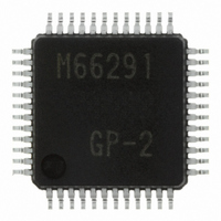
M66291GP#201 Renesas Electronics America, M66291GP#201 Datasheet - Page 5

M66291GP#201
Manufacturer Part Number
M66291GP#201
Description
IC USB CONTROLLER GEN-PUR 48LQFP
Manufacturer
Renesas Electronics America
Datasheet
1.M66291GP201.pdf
(126 pages)
Specifications of M66291GP#201
Package / Case
48-LQFP
Mounting Type
Surface Mount
Current - Supply
30mA
Voltage - Supply
3 V ~ 3.6 V
Operating Temperature
-20°C ~ 85°C
Interface
Serial
Controller Type
USB 2.0 Controller
Lead Free Status / RoHS Status
Not Compliant
Available stocks
Company
Part Number
Manufacturer
Quantity
Price
M 6 6 2 9 1 G P / H P
1.2.1
1.2.2
1.2.3
1.2.4
R e v 1 . 0 1
(2) Transfer Controller
(1) Serial Interface Engine (SIE)
(3) Endpoint Controller
(4) FIFO Memory Controller
(5) Interrupt Controller
(6) CPU Interface Register
The USB-IP block contains a serial interface engine, a transfer controller, an endpoint controller, a FIFO
memory controller, an interrupt controller, and a CPU interface register.
The serial interface engine (SIE) executes low-order protocols processing of USB as follows:
The transfer controller executes device state transition control and control transfer sequence control.
The endpoint controller executes status control per endpoint.
The FIFO memory controller controls the write/read of the transmit/receive data at SIE (USB bus) side and
internal bus (CPU bus) side under state control by the endpoint controller.
The interrupt controller outputs the status signals outputted by transfer controller and endpoint controller to
INT0, INT1/SOF interrupt pins according to the CPU interface register setting.
The CPU interface register block is composed of the registers for mode setting, command setting and status
reading.
The bus interface unit (BIU) is a circuit to conform USB-IP to LSI external bus.
The FIFO memory is a FIFO for endpoint transmit/receive. It is possible to set 6 endpoints EP1 to EP6 in
addition to EP0, the endpoint for control transfer.
The I/O block is composed of USB transceiver, oscillation buffer, 48 MHz PLL, Vbus input circuit and D+ pin
pullup control circuit.
USB-IP
Bus Interface Unit (BIU)
FIFO Memory
I/O Block
2 0 0 4 . 1 1 . 0 1
•
•
•
•
•
•
•
Extracts receive data/clock and generates transmit clock
Serial - parallel conversion of transmit/receive data
NRZI (Non Return Zero Invert) encoding and decoding
Bit stuffing and destuffing
SYNC (Synchronization pattern) and EOP (End Of Packet) detection
USB address and endpoint detection
CRC (Cyclic Redundancy Check) generation and checking
p a g e 5 o f 1 2 2


