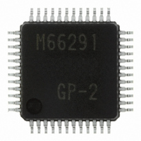
M66291GP#201 Renesas Electronics America, M66291GP#201 Datasheet - Page 98

M66291GP#201
Manufacturer Part Number
M66291GP#201
Description
IC USB CONTROLLER GEN-PUR 48LQFP
Manufacturer
Renesas Electronics America
Datasheet
1.M66291GP201.pdf
(126 pages)
Specifications of M66291GP#201
Package / Case
48-LQFP
Mounting Type
Surface Mount
Current - Supply
30mA
Voltage - Supply
3 V ~ 3.6 V
Operating Temperature
-20°C ~ 85°C
Interface
Serial
Controller Type
USB 2.0 Controller
Lead Free Status / RoHS Status
Not Compliant
Available stocks
Company
Part Number
Manufacturer
Quantity
Price
M 6 6 2 9 1 G P / H P
3.5.1
3.5.2
R e v 1 . 0 1
FIFO Buffer Management
Cautions at FIFO Data Access
B-2) 8-bit mode (Octl bit =“1”)
The M66291 is equipped with the registers below in order to execute high-level management of the FIFO
buffer set to continuous transmit/receive mode.
(1) SIE_FIFO Status Register
(2) Transaction Count Register
(3) FIFO Status Register
Make sure of the items as follows when accessing the FIFO Data Register.
When 8-bit width is selected in CPU interface:
When 16-bit width is selected in CPU interface:
B-1) 16-bit mode (Octl bit =“0”)
2 0 0 4 . 1 1 . 0 1
The FIFO data can be set both to 16-bit and 8-bit modes by the register bit (Octl).
The FIFO data can not be set to 16-bit mode by the register bit (Octl), while *LWR pin becomes valid as the
write strobe at 8-bit mode.
This register is used for referring to the FIFO buffer status.
This register can forcibly toggle the FIFO buffer at SIE side of double buffer, enabling the CPU to access to
the SIE side FIFO. Further, the CPU can refer to the received data number in the SIE side FIFO.
When the continuous transfer mode buffer set in the OUT bulk transfer, the data receive count by MAX
packet size is specified, enabling the transaction only for the set count. It is convenient for the DMA
transfer.
When accessing data for write, *LWR pin is valid as the write strobe. Here, D7 to 0 become valid.
When accessing data for read, D15 to 8 and D7 to 0 are the same.
When accessing data for write, assert *HWR and *LWR pins simultaneously for word access, and *LWR
pin for byte access. At byte access, D7 to 0 become valid.
p a g e 9 8 o f 1 2 2


