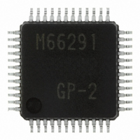
M66291GP#201 Renesas Electronics America, M66291GP#201 Datasheet - Page 55

M66291GP#201
Manufacturer Part Number
M66291GP#201
Description
IC USB CONTROLLER GEN-PUR 48LQFP
Manufacturer
Renesas Electronics America
Datasheet
1.M66291GP201.pdf
(126 pages)
Specifications of M66291GP#201
Package / Case
48-LQFP
Mounting Type
Surface Mount
Current - Supply
30mA
Voltage - Supply
3 V ~ 3.6 V
Operating Temperature
-20°C ~ 85°C
Interface
Serial
Controller Type
USB 2.0 Controller
Lead Free Status / RoHS Status
Not Compliant
Available stocks
Company
Part Number
Manufacturer
Quantity
Price
M 6 6 2 9 1 G P / H P
R e v 1 . 0 1
(2) RWND (Buffer Rewind) Bit (b12)
(3) BSWP (Byte Swap Mode) Bit (b7)
(4) Octl (Register 8-Bit Mode) Bit (b6)
(5) CPU_EP (CPU Access Endpoint Designate) Bits (b3~b0)
This bit rewinds (initializes) the buffer pointer.
This bit sets the endian of the CPU_FIFO Data Register.
When this bit is set to “0”, the CPU_FIFO Data Register gets such as little endian.
When this bit is set to “1”, the CPU_FIFO Data Register gets such as big endian.
This bit sets the access mode of the CPU_FIFO Data Register.
When this bit is set to “0”, the CPU_FIFO Data Register is set to 16-bit mode, and all bits of the CPU_FIFO
Data Register are valid.
When this bit is set to “1”, the CPU_FIFO Data Register is set to 8-bit mode, and the upper-order 8 bits of the
CPU_FIFO Data Register (b15 to b8) are invalid.
When set to OUT buffer (EPi_DIR bit = “0”), change this bit before receiving the data. When set to IN buffer
(EPi_DIR bit = “1”), if the Creq bit is equal to “1”, do not change this bit.
This bit becomes invalid (fixed to 8-bit mode) when the mode is set to 8-bit by *HWR/*BYTE pin.
In such case, this bit is read “0”.
These bits select the endpoint accessed by CPU.
Make sure that the endpoint selection does not get overlapped with the selection by the DMA_EP bits.
When making a change in these bits to select the other the endpoint, make sure that the source endpoint and
the destination endpoint to be changed are not under the access by the CPU or during receiving/transmitting
of SIE (under access to FIFO buffer).
2 0 0 4 . 1 1 . 0 1
Note:
Note:
When set to OUT buffer (EPi_DIR bit = “0”)
When set to IN buffer (EPi_DIR bit = “1”)
When the IVAL bit of the CPU_FIFO Control Register is set to “1”, the buffer reading pointer can be
initialized by writing “1” to this bit. This enables reading of the receive data from the beginning.
When the IVAL bit of the CPU_FIFO Control Register is set to “0”, the buffer writing pointer can be
initialized by writing “1” to this bit. This enables resetting of the transmit data from the beginning.
The operation is equivalent to the case when “1” is set to the BCLR bit if set to IN buffer.
Do not set this bit to “1” when the mode is set to 8-bit (set by the Octl bit or *HWR/*BYTE pin).
The access width of the CPU_FIFO Data Register is controlled by the logical sum of this bit and the EPi_Octl
bits of the EPi Configuration Register 1 specified by the CPU_EP bits. Hence, the mode is set to 8-bit if “1” is
set to either this bit or to the EPi_Octl bits of the EPi Configuration Register 1. Make sure that both bits must be
set to “0” to change to 16-bit mode.
p a g e 5 5 o f 1 2 2
Little Endian
Big Endian
even number address
odd number address
b15~b8
even number address
odd number address
b7~b0


