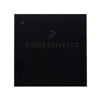
DSP56301VF100 Freescale, DSP56301VF100 Datasheet - Page 19

DSP56301VF100
Manufacturer Part Number
DSP56301VF100
Description
Manufacturer
Freescale
Datasheet
1.DSP56301VF100.pdf
(124 pages)
Specifications of DSP56301VF100
Device Core Size
24b
Format
Fixed Point
Clock Freq (max)
100MHz
Mips
100
Device Input Clock Speed
100MHz
Ram Size
24KB
Operating Supply Voltage (typ)
3.3V
Operating Supply Voltage (min)
3V
Operating Supply Voltage (max)
3.6V
Operating Temp Range
-40C to 100C
Operating Temperature Classification
Industrial
Mounting
Surface Mount
Pin Count
252
Package Type
MA-BGA
Lead Free Status / RoHS Status
Not Compliant
Available stocks
Company
Part Number
Manufacturer
Quantity
Price
Company:
Part Number:
DSP56301VF100
Manufacturer:
Freescale Semiconductor
Quantity:
10 000
Part Number:
DSP56301VF100
Manufacturer:
MOTOROLA/摩托罗拉
Quantity:
20 000
Freescale Semiconductor
HCLK
HAD[16–31]
HD[8–23]
HRST
HRST
HINTA
PVCL
Signal Name
Input
Input/Output
Input/Output
Input
Input
Output, open
drain
Input
Type
Input
Tri-stated
Tri-stated
Tri-stated
Input
State During
Table 1-11.
Reset
DSP56301 Technical Data, Rev. 10
Host Clock
When the HI32 is programmed to interface with a PCI bus and the HI function
is selected, this is the Host Bus Clock input.
Non-PCI bus
When HI32 is programmed to interface a universal non-PCI bus and the HI
function is selected, this signal must be connected to a pull-up resistor or
directly to V
Port B
When the HI32 is configured as GPIO through the DCTR, this signal is
internally disconnected.
This input is 5 V tolerant.
Host Address/Data 16–31
When the HI32 is programmed to interface with a PCI bus and the HI function
is selected, these signals are lines 16–31 of the Address/Data bus.
Host Data 8–23
When HI32 is programmed to interface with a universal, non-PCI bus and the
HI function is selected, these signals are lines 8–23 of the Data bus.
Port B
When the HI32 is configured as GPIO through the DCTR, these signals are
internally disconnected.
These inputs are 5 V tolerant.
Hardware Reset
When the HI32 is programmed to interface with a PCI bus and the HI function
is selected, this is the Hardware Reset input.
Hardware Reset
When HI32 is programmed to interface with a universal, non-PCI bus and the
HI function is selected, this is the Hardware Reset Schmitt-trigger signal.
Port B
When the HI32 is configured as GPIO through the DCTR, this signal is
internally disconnected.
This input is 5 V tolerant.
Host Interrupt A
When the HI function is selected, this signal is the Interrupt A open-drain
output.
Port B
When the HI32 is configured as GPIO through the DCTR, this signal is
internally disconnected.
This input is 5 V tolerant.
PCI Voltage Clamp
When the HI32 is programmed to interface with a PCI bus and the HI function
is selected and the PCI bus uses a 3 V signal environment, connect this pin to
V
specifications. In all other cases, including a 5 V PCI signal environment, leave
the input unconnected.
Host Interface (Continued)
CC
(3.3 V) to enable the high voltage clamping required by the PCI
CC
.
Signal Description
Host Interface (HI32)
1-15


