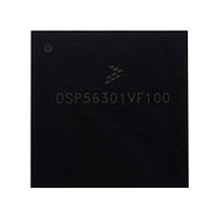
DSP56301VF100 Freescale, DSP56301VF100 Datasheet - Page 50

DSP56301VF100
Manufacturer Part Number
DSP56301VF100
Description
Manufacturer
Freescale
Datasheet
1.DSP56301VF100.pdf
(124 pages)
Specifications of DSP56301VF100
Device Core Size
24b
Format
Fixed Point
Clock Freq (max)
100MHz
Mips
100
Device Input Clock Speed
100MHz
Ram Size
24KB
Operating Supply Voltage (typ)
3.3V
Operating Supply Voltage (min)
3V
Operating Supply Voltage (max)
3.6V
Operating Temp Range
-40C to 100C
Operating Temperature Classification
Industrial
Mounting
Surface Mount
Pin Count
252
Package Type
MA-BGA
Lead Free Status / RoHS Status
Not Compliant
Available stocks
Company
Part Number
Manufacturer
Quantity
Price
Company:
Part Number:
DSP56301VF100
Manufacturer:
Freescale Semiconductor
Quantity:
10 000
Part Number:
DSP56301VF100
Manufacturer:
MOTOROLA/摩托罗拉
Quantity:
20 000
Specifications
2-24
Notes:
157
No.
No.
187
188
189
190
191
192
193
194
195
158
159
160
161
162
163
164
165
166
167
168
169
RAS assertion to data not valid (write)
WR assertion to CAS assertion
CAS assertion to RAS assertion (refresh)
RAS deassertion to CAS assertion (refresh)
RD assertion to RAS deassertion
RD assertion to data valid
RD deassertion to data not valid
WR assertion to data active
WR deassertion to data high impedance
Random read or write cycle time
RAS assertion to data valid (read)
CAS assertion to data valid (read)
Column address valid to data valid (read)
CAS deassertion to data not valid (read hold time)
RAS deassertion to RAS assertion
RAS assertion pulse width
CAS assertion to RAS deassertion
RAS assertion to CAS deassertion
CAS assertion pulse width
RAS assertion to CAS assertion
RAS assertion to column address valid
CAS deassertion to RAS assertion
1.
2.
3.
4.
Table 2-13.
The number of wait states for an out-of-page access is specified in the DCR.
The refresh period is specified in the DCR.
RD deassertion always occurs after CAS deassertion; therefore, the restricted timing is t
Either t
Table 2-14.
RCH
Characteristics
Characteristics
or t
RRH
DRAM Out-of-Page and Refresh Timings, Eleven Wait States
must be satisfied for read cycles.
3
DRAM Out-of-Page and Refresh Timings, Fifteen Wait States
3
3
DSP56301 Technical Data, Rev. 10
Symbol
Symbol
t
t
t
t
t
t
t
t
t
t
t
t
t
t
t
WCS
ROH
DHR
CSR
RPC
t
t
t
RAC
CAC
t
OFF
t
RAS
RSH
CSH
CAS
RCD
RAD
CRP
GA
GZ
RC
RP
AA
7.75 × T
2.75 × T
11.5 × T
0.75 × T
8.25 × T
8.25 × T
4.75 × T
4.75 × T
6.25 × T
9.75 × T
6.25 × T
8.25 × T
4.75 × T
2.75 × T
7.75 × T
Expression
6.5 × T
1.5 × T
Expression
5.5 × T
5.5 × T
10 × T
10 × T
3.5 × T
100 MHz:
0.25 × T
100 MHz:
100 MHz:
100 MHz:
80 MHz:
80 MHz:
80 MHz:
80 MHz:
16 × T
0.0
C
C
C
C
C
C
C
C
C
C
C
C
C
C
C
C
C
C
C
C
C
C
− 6.5
− 7.0
− 4.3
− 4.0
− 6.5
− 5.7
− 4.0
− 4.0
− 4.0
– 1.5
C
− 6.5
− 5.7
− 6.5
− 5.7
− 4.0
− 4.0
− 4.0
− 4.0
− 4.0
± 2.0
− 4.0
± 2
C
139.8
200.0
117.9
92.9
77.0
14.8
30.4
74.1
74.1
99.1
55.4
41.8
32.4
92.9
Min
Min
OFF
0.0
9.1
0.0
—
—
—
—
—
—
—
—
—
80 MHz
80 MHz
and not t
1, 2
118.5
Max
Max
96.6
52.9
62.3
45.8
36.4
3.1
—
—
—
—
—
—
—
—
—
—
—
—
—
—
—
—
—
—
—
(Continued)
Freescale Semiconductor
1, 2
GZ
.
111.0
160.0
Min
73.5
60.7
11.0
23.5
Min
58.5
93.5
58.5
78.5
43.5
33.0
25.5
73.5
0.0
6.0
0.0
—
—
—
—
—
—
—
—
—
100 MHz
100 MHz
Max
Max
93.0
76.8
41.8
49.3
37.0
29.5
2.5
—
—
—
—
—
—
—
—
—
—
—
—
—
—
—
—
—
—
—
Unit
Unit
ns
ns
ns
ns
ns
ns
ns
ns
ns
ns
ns
ns
ns
ns
ns
ns
ns
ns
ns
ns
ns
ns
ns
ns
ns
ns


