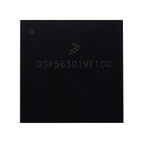
DSP56301VF100 Freescale, DSP56301VF100 Datasheet - Page 54

DSP56301VF100
Manufacturer Part Number
DSP56301VF100
Description
Manufacturer
Freescale
Datasheet
1.DSP56301VF100.pdf
(124 pages)
Specifications of DSP56301VF100
Device Core Size
24b
Format
Fixed Point
Clock Freq (max)
100MHz
Mips
100
Device Input Clock Speed
100MHz
Ram Size
24KB
Operating Supply Voltage (typ)
3.3V
Operating Supply Voltage (min)
3V
Operating Supply Voltage (max)
3.6V
Operating Temp Range
-40C to 100C
Operating Temperature Classification
Industrial
Mounting
Surface Mount
Pin Count
252
Package Type
MA-BGA
Lead Free Status / RoHS Status
Not Compliant
Available stocks
Company
Part Number
Manufacturer
Quantity
Price
Company:
Part Number:
DSP56301VF100
Manufacturer:
Freescale Semiconductor
Quantity:
10 000
Part Number:
DSP56301VF100
Manufacturer:
MOTOROLA/摩托罗拉
Quantity:
20 000
Specifications
2.5.5.3 Synchronous Timings (SRAM)
2-28
Notes:
No.
196
197
198
199
200
201
202
203
204
205
206
207
208
209
210
211
CLKOUT high to BS assertion
CLKOUT high to BS deassertion
CLKOUT high to address, and AA valid
CLKOUT high to address, and AA invalid
TA valid to CLKOUT high (setup time)
CLKOUT high to TA invalid (hold time)
CLKOUT high to data out active
CLKOUT high to data out valid
CLKOUT high to data out invalid
CLKOUT high to data out high impedance
Data in valid to CLKOUT high (setup)
CLKOUT high to data in invalid (hold)
CLKOUT high to RD assertion
CLKOUT high to RD deassertion
CLKOUT high to WR assertion
CLKOUT high to WR deassertion
1.
2.
3.
4.
WS is the number of wait states specified in the BCR.
If WS > 1, WR assertion refers to the next rising edge of CLKOUT.
External bus synchronous timings should be used only for reference to the clock and not for relative timings.
T198 and T199 are valid for Address Trace mode if the ATE bit in the Operating Mode Register is set. Use the status of BR
(See T212) to determine whether the access referenced by A[0–23] is internal or external in this mode.
Characteristics
Table 2-15.
2
External Bus Synchronous Timings (SRAM Access)
4
DSP56301 Technical Data, Rev. 10
4
0.25 × T
0.75 × T
[WS = 1 or WS ≥ 4]
Expression
0.25 × T
0.25 × T
0.25 × T
0.25 × T
0.25 × T
0.75 × T
0.5 × T
[2 ≤ WS ≤ 3]
maximum:
0.25 × T
100 MHz:
0.25 × T
100 MHz:
0.25 × T
80 MHz:
80 MHz:
C
C
C
+5.2/–0.5
+4.2/–1.0
C
C
C
C
C
C
+ 4.3
+ 2.5
– 0.7
+ 4.5
+ 4.0
+ 0.5
+ 2.5
C
C
C
1,2
Min
10.4
2.6
8.4
2.4
5.8
0.0
3.1
3.1
5.0
0.0
0.0
7.6
1.3
0.0
—
—
—
—
—
80 MHz
Max
13.6
11.9
10.6
8.3
5.6
7.6
3.6
4.5
4.8
4.3
—
—
—
—
—
—
—
—
—
3
Freescale Semiconductor
Min
2.0
6.5
1.8
4.0
0.0
2.5
2.5
4.0
0.0
6.7
0.0
4.5
0.0
0.0
—
—
—
—
—
100 MHz
Max
11.7
10.0
7.7
5.0
6.5
2.5
4.0
9.3
4.3
3.8
—
—
—
—
—
—
—
—
—
Unit
ns
ns
ns
ns
ns
ns
ns
ns
ns
ns
ns
ns
ns
ns
ns
ns
ns
ns
ns
ns


