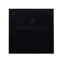
DSP56301VF100 Freescale, DSP56301VF100 Datasheet - Page 28

DSP56301VF100
Manufacturer Part Number
DSP56301VF100
Description
Manufacturer
Freescale
Datasheet
1.DSP56301VF100.pdf
(124 pages)
Specifications of DSP56301VF100
Device Core Size
24b
Format
Fixed Point
Clock Freq (max)
100MHz
Mips
100
Device Input Clock Speed
100MHz
Ram Size
24KB
Operating Supply Voltage (typ)
3.3V
Operating Supply Voltage (min)
3V
Operating Supply Voltage (max)
3.6V
Operating Temp Range
-40C to 100C
Operating Temperature Classification
Industrial
Mounting
Surface Mount
Pin Count
252
Package Type
MA-BGA
Lead Free Status / RoHS Status
Not Compliant
Available stocks
Company
Part Number
Manufacturer
Quantity
Price
Company:
Part Number:
DSP56301VF100
Manufacturer:
Freescale Semiconductor
Quantity:
10 000
Part Number:
DSP56301VF100
Manufacturer:
MOTOROLA/摩托罗拉
Quantity:
20 000
Specifications
2.2 Absolute Maximum Ratings
2.3 Thermal Characteristics
2.4 DC Electrical Characteristics
2-2
Supply voltage
Supply Voltage
All input voltages excluding “5 V tolerant” inputs
All “5 V tolerant” input voltages
Current drain per pin excluding V
Operating temperature range
Storage temperature
Notes:
Junction-to-ambient thermal resistance
Junction-to-case thermal resistance
Thermal characterization parameter
Notes:
1.
2.
3.
1.
2.
3.
4.
GND = 0 V, V
Absolute maximum ratings are stress ratings only, and functional operation at the maximum is not guaranteed. Stress
beyond the maximum rating may affect device reliability or cause permanent damage to the device.
CAUTION: All “5 V Tolerant” input voltages cannot be more than 3.95 V greater than the supply voltage; this restriction
applies to “power on,” as well as during normal operation. In any case, the input voltages must not be higher than 5.75 V. “5
V Tolerant” inputs are inputs that tolerate 5 V.
Junction-to-ambient thermal resistance is based on measurements on a horizontal single-sided printed circuit board per
JEDEC Specification JESD51-3.
Junction-to-case thermal resistance is based on measurements using a cold plate per SEMI G30-88, with the exception that
the cold plate temperature is used for the case temperature.
These are simulated values. See note 1 for test board conditions.
These are simulated values. The test board has two 2-ounce signal layers and two 1-ounce solid ground planes internal to
the test board.
Characteristics
Characteristic
CC
Rating
3
= 3.3 V ± 0.3 V, T
CC
2
and GND
1
1
Table 2-3.
Table 2-2.
3
DSP56301 Technical Data, Rev. 10
Table 2-1.
J
= –40°C to +100°C, CL = 50 pF
DC Electrical Characteristics
Symbol
Thermal Characteristics
V
CC
Maximum Ratings
R
R
Symbol
θJC
θJA
Ψ
or θ
or θ
JT
Symbol
JA
JC
T
V
V
V
T
STG
IN5
CC
I
IN
Min
J
3.0
TQFP
Value
49.5
7.2
4.7
6
GND – 0.3 to V
GND – 0.3 to V
PBGA
Typ
Value
3.3
48.4
–0.3 to +4.0
–40 to +100
–55 to +150
Value
9
5
10
3
1, 2
CC
CC
Freescale Semiconductor
+ 3.95
+ 0.3
PBGA
Value
25.2
—
—
Max
3.6
4
°
°
°
Unit
Unit
mA
°
°
C/W
C/W
C/W
Unit
V
V
V
C
C
V


