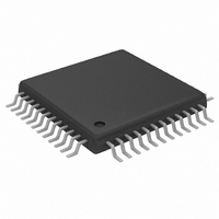
MAX1196ECM+D Maxim Integrated Products, MAX1196ECM+D Datasheet - Page 11

MAX1196ECM+D
Manufacturer Part Number
MAX1196ECM+D
Description
IC ADC 8BIT 40MSPS DL 48-TQFP
Manufacturer
Maxim Integrated Products
Datasheet
1.MAX1196ECMD.pdf
(23 pages)
Specifications of MAX1196ECM+D
Number Of Bits
8
Sampling Rate (per Second)
40M
Data Interface
Parallel
Number Of Converters
2
Power Dissipation (max)
108mW
Voltage Supply Source
Single Supply
Operating Temperature
-40°C ~ 85°C
Mounting Type
Surface Mount
Package / Case
48-TQFP Exposed Pad, 48-eTQFP, 48-HTQFP, 48-VQFP
Lead Free Status / RoHS Status
Lead free / RoHS Compliant
Internal Reference and Multiplexed Parallel Outputs
21–29, 35, 36
31, 34
32, 33
PIN
17
18
19
20
30
37
38
39
40
41
42
43
44
45
46
47
48
Dual 8-Bit, 40Msps, 3V, Low-Power ADC with
REFOUT Internal Reference Voltage Output. Can be connected to REFIN through a resistor or a resistor-divider.
SLEEP
OGND
NAME
D0A/B
D1A/B
D2A/B
D3A/B
D4A/B
D5A/B
D6A/B
D7A/B
REFIN
OV
REFN
REFP
N.C.
A/B
T/B
OE
PD
______________________________________________________________________________________
DD
T/B selects the ADC digital output format.
High: Two’s complement.
Low: Straight offset binary.
Sleep Mode Input.
High: Deactivates the two ADCs, but leaves the reference bias circuit active.
Low: Normal operation.
High-Active Power-Down Input.
High: Power-down mode
Low: Normal operation
Low-Active Output Enable Input.
High: Digital outputs disabled
Low: Digital outputs enabled
No Connection. Do not connect.
A/B Data Indicator. This digital output indicates CHA data (A/B = 1) or CHB data (A/B = 0) to be
present on the output. A/B follows the external clock signal with typically 6ns delay.
Output-Driver Ground
Output-Driver Supply Voltage. Bypass to OGND with a capacitor combination of 2.2µF in parallel with
0.1µF.
Three-State Digital Output, Bit 0. Depending on status of A/B, output data reflects channel A or
channel B data.
Three-State Digital Output, Bit 1. Depending on status of A/B, output data reflects channel A or
channel B data.
Three-State Digital Output, Bit 2. Depending on status of A/B, output data reflects channel A or
channel B data.
Three-State Digital Output, Bit 3. Depending on status of A/B, output data reflects channel A or
channel B data.
Three-State Digital Output, Bit 4. Depending on status of A/B, output data reflects channel A or
channel B data.
Three-State Digital Output, Bit 5. Depending on status of A/B, output data reflects channel A or
channel B data.
Three-State Digital Output, Bit 6. Depending on status of A/B, output data reflects channel A or
channel B data.
Three-State Digital Output, Bit 7 (MSB). Depending on status of A/B, output data reflects channel A or
channel B data.
Reference Input. V
Positive Reference I/O. Conversion range is ±(V
Negative Reference I/O. Conversion range is ±(V
capacitor.
REFIN
= 2 × (V
REFP
- V
REFN
). Bypass to GND with a ≥0.1µF capacitor.
FUNCTION
REFP
REFP
- V
Pin Description (continued)
- V
REFN
REFN
). Bypass to GND with a ≥0.1µF capacitor.
). Bypass to GND with a ≥0.1µF
11


