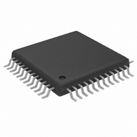
MAX1196ECM+D Maxim Integrated Products, MAX1196ECM+D Datasheet - Page 12

MAX1196ECM+D
Manufacturer Part Number
MAX1196ECM+D
Description
IC ADC 8BIT 40MSPS DL 48-TQFP
Manufacturer
Maxim Integrated Products
Datasheet
1.MAX1196ECMD.pdf
(23 pages)
Specifications of MAX1196ECM+D
Number Of Bits
8
Sampling Rate (per Second)
40M
Data Interface
Parallel
Number Of Converters
2
Power Dissipation (max)
108mW
Voltage Supply Source
Single Supply
Operating Temperature
-40°C ~ 85°C
Mounting Type
Surface Mount
Package / Case
48-TQFP Exposed Pad, 48-eTQFP, 48-HTQFP, 48-VQFP
Lead Free Status / RoHS Status
Lead free / RoHS Compliant
The MAX1196 uses a 7-stage, fully differential, pipelined
architecture (Figure 1) that allows for high-speed con-
version while minimizing power consumption. Samples
taken at the inputs move progressively through the
pipeline stages every half clock cycle. Including the
delay through the output latch, the total clock-cycle
latency is 5 clock cycles for CHA and 5.5 clock cycles
for CHB.
Flash ADCs convert the held input voltages into a digi-
tal code. Internal MDACs convert the digitized results
back into analog voltages, which are then subtracted
from the original held input signals. The resulting error
signals are then multiplied by two, and the residues are
passed along to the next pipeline stages where the
process is repeated until the signals have been
processed by all 7 stages.
Both input channels are sampled on the rising edge of
the clock and the resulting data is multiplexed at the
output. CHA data is updated on the rising edge (5
clock cycles later) and CHB data is updated on the
falling edge (5.5 clock cycles later) of the clock signal.
The A/B indicator follows the clock signal with a typical
delay time of 6ns and remains high when CHA data is
updated and low when CHB data is updated.
Figure 2 displays a simplified functional diagram of the
input track-and-hold (T/H) circuits in both track and
hold mode. In track mode, switches S1, S2a, S2b, S4a,
Dual 8-Bit, 40Msps, 3V, Low-Power ADC with
Internal Reference and Multiplexed Parallel Outputs
Figure 1. Pipelined Architecture—Stage Blocks
12
V
INA
______________________________________________________________________________________
T/H
Input Track-and-Hold (T/H) Circuits
STAGE 1
DIGITAL ALIGNMENT LOGIC
Detailed Description
STAGE 2
8
STAGE 6
2-BIT FLASH
STAGE 7
OUTPUT MULTIPLEXER
ADC
8
D0A/B–D7A/B
S4b, S5a, and S5b are closed. The fully differential cir-
cuits sample the input signals onto the two capacitors
(C2a and C2b) through switches S4a and S4b. S2a and
S2b set the common mode for the amplifier input, and
open simultaneously with S1, sampling the input wave-
form. Switches S4a, S4b, S5a, and S5b are then
opened before switches S3a and S3b connect capaci-
tors C1a and C1b to the output of the amplifier and
switch S4c is closed. The resulting differential voltages
are held on capacitors C2a and C2b. The amplifiers are
used to charge capacitors C1a and C1b to the same
values originally held on C2a and C2b. These values
are then presented to the first stage quantizers and iso-
late the pipelines from the fast-changing inputs. The
wide input bandwidth T/H amplifiers allow the MAX1196
to track and sample/hold analog inputs of high frequen-
cies (>Nyquist). Both ADC inputs (INA+, INB+, INA-,
and INB-) can be driven either differentially or single
ended. Match the impedance of INA+ and INA-, as well
as INB+ and INB-, and set the common-mode voltage
to midsupply (V
The full-scale range of the MAX1196 is determined by
the internally generated voltage difference between
REFP (V
The full-scale range for both on-chip ADCs is
adjustable through the REFIN pin, which is provided for
this purpose.
V
INB
T/H
DD
STAGE 1
/2 + V
DD
DIGITAL ALIGNMENT LOGIC
REFIN
Analog Inputs and Reference
/2) for optimum performance.
STAGE 2
/4) and REFN (V
8
STAGE 6
Configurations
DD
/2 - V
2-BIT FLASH
REFIN
STAGE 7
ADC
/4).


