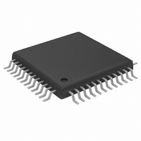
MAX1196ECM+D Maxim Integrated Products, MAX1196ECM+D Datasheet - Page 14

MAX1196ECM+D
Manufacturer Part Number
MAX1196ECM+D
Description
IC ADC 8BIT 40MSPS DL 48-TQFP
Manufacturer
Maxim Integrated Products
Datasheet
1.MAX1196ECMD.pdf
(23 pages)
Specifications of MAX1196ECM+D
Number Of Bits
8
Sampling Rate (per Second)
40M
Data Interface
Parallel
Number Of Converters
2
Power Dissipation (max)
108mW
Voltage Supply Source
Single Supply
Operating Temperature
-40°C ~ 85°C
Mounting Type
Surface Mount
Package / Case
48-TQFP Exposed Pad, 48-eTQFP, 48-HTQFP, 48-VQFP
Lead Free Status / RoHS Status
Lead free / RoHS Compliant
Dual 8-Bit, 40Msps, 3V, Low-Power ADC with
Internal Reference and Multiplexed Parallel Outputs
and REFN are outputs. REFOUT can be left open or
connected to REFIN through a >10kΩ resistor.
In unbuffered external reference mode, connect REFIN
to GND. This deactivates the on-chip reference buffers
for REFP, COM, and REFN. With their buffers shut down,
these nodes become high-impedance inputs and can be
driven through separate, external reference sources.
For detailed circuit suggestions and how to drive this
dual ADC in buffered/unbuffered external reference
mode, see the Applications Information section.
The MAX1196’s CLK input accepts CMOS-compatible
clock signal. Since the interstage conversion of the
device depends on the repeatability of the rising and
falling edges of the external clock, use a clock with low
jitter and fast rise and fall times (<2ns). In particular,
sampling occurs on the rising edge of the clock signal,
requiring this edge to provide lowest possible jitter. Any
significant aperture jitter would limit the SNR perfor-
mance of the on-chip ADCs as follows:
where f
t
Figure 3. System Timing Diagram
14
AJ
CHB
D0A/B–D7A/B
CLK
t
CHA
is the time of the aperture jitter.
t
DA/B
A/B
DOB
______________________________________________________________________________________
IN
SNR
represents the analog input frequency and
t
CL
CHB
D0B
t
=
CLK
20
t
CH
CHA
D1A
×
log
t
DOA
CHB
D1B
2 π
× ×
Clock Input (CLK)
5 CLOCK-CYCLE LATENCY (CHA), 5.5 CLOCK-CYCLE LATENCY (CHB)
CHA
D2A
f
1
IN
×
t
AJ
CHB
D2B
CHA
D3A
CHB
D3B
Clock jitter is especially critical for undersampling
applications. The clock input should always be consid-
ered as an analog input and routed away from any ana-
log input or other digital signal lines.
The MAX1196 clock input operates with a voltage
threshold set to V
other than 50%, must meet the specifications for high
and low periods as stated in the Electrical
Characteristics.
Figure 3 shows the relationship between clock and
analog input, A/B indicator, and the resulting valid
CHA/CHB data output. CHA and CHB data are sam-
pled on the rising edge of the clock signal. Following
the rising edge of the 5th clock cycles, the digitized
value of the original CHA sample is presented at the
output, followed one-half clock cycle later by the digi-
tized value of the original CHB sample.
A channel selection signal (A/B indicator) allows the
user to determine which output data represents which
input channel. With A/B = 1, digitized data from CHA is
present at the output and with A/B = 0 digitized data
from CHB is present.
CHA
D4A
CHB
D4B
System Timing Requirements
DD
/2. Clock inputs with a duty cycle
CHA
D5A
CHB
D5B
CHA
D6A
CHB
D6B


