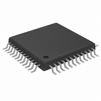
MAX1196ECM+D Maxim Integrated Products, MAX1196ECM+D Datasheet - Page 4

MAX1196ECM+D
Manufacturer Part Number
MAX1196ECM+D
Description
IC ADC 8BIT 40MSPS DL 48-TQFP
Manufacturer
Maxim Integrated Products
Datasheet
1.MAX1196ECMD.pdf
(23 pages)
Specifications of MAX1196ECM+D
Number Of Bits
8
Sampling Rate (per Second)
40M
Data Interface
Parallel
Number Of Converters
2
Power Dissipation (max)
108mW
Voltage Supply Source
Single Supply
Operating Temperature
-40°C ~ 85°C
Mounting Type
Surface Mount
Package / Case
48-TQFP Exposed Pad, 48-eTQFP, 48-HTQFP, 48-VQFP
Lead Free Status / RoHS Status
Lead free / RoHS Compliant
Dual 8-Bit, 40Msps, 3V, Low-Power ADC with
Internal Reference and Multiplexed Parallel Outputs
ELECTRICAL CHARACTERISTICS (continued)
(V
resistor, V
unless otherwise noted. ≥+25°C guaranteed by production test, <+25°C guaranteed by design and characterization. Typical values
are at T
4
BUFFERED EXTERNAL REFERENCE (V
Positive Reference Output
Voltage
Negative Reference Output
Voltage
Common-Mode Level
Differential Reference Output
Voltage Range
REFIN Resistance
Maximum REFP, COM Source
Current
Maximum REFP, C OM S i nk C ur r ent
Maximum REFN Source Current
Maximum REFN Sink Current
UNBUFFERED EXTERNAL REFERENCE (V
REFP, REFN Input Resistance
REFP, REFN, COM Input
Capacitance
Differential Reference Input
Voltage Range
COM Input Voltage Range
REFP Input Voltage
REFN Input Voltage
DIGITAL INPUTS (CLK, PD, OE, SLEEP, T/B)
Input High Threshold
Input Low Threshold
DD
_______________________________________________________________________________________
= OV
A
= +25°C.)
IN
DD
PARAMETER
= 2V
= 3V, 0.1µF and 2.2µF capacitors from REFP, REFN, and COM to GND; REFOUT connected to REFIN through a 10kΩ
P-P
(differential with respect to COM), C
SYMBOL
I
I
SOURCE
SOURCE
R
R
V
∆V
R
∆V
V
V
V
V
V
I
I
REFIN
REFP
REFN
SINK
SINK
C
REFN
REFP
REFN
REFP
V
COM
COM
V
REF
REF
IN
IH
IL
REFIN
,
REFIN
= 2.048V)
(Note 5)
(Note 5)
(Note 5)
∆V
Measured between REFP and REFN
∆V
CLK
PD, OE, SLEEP, T/B
CLK
PD, OE, SLEEP, T/B
= AGND, reference voltage applied to REFP, REFN, and COM)
REF
REF
= V
= V
L
REFP
REFP
= 10pF at digital outputs (Note 5), f
CONDITIONS
- V
- V
REFN
REFN
OV
0.8 ×
CLK
MIN
0.8 ×
V
DD
DD
= 40MHz, T
∆V
∆V
V
V
V
V
1.024
±10%
2.012
0.988
1.024
C OM
COM
DD
±2%
-250
DD
±5%
REF
TYP
±0.1
>50
250
RE F
15
-5
4
5
/ 2
/ 2
/ 2
/ 2
+
-
A
OV
0.2 ×
0.2 ×
MAX
V
= T
DD
DD
MIN
to T
UNITS
MΩ
mA
mA
kΩ
µA
µA
pF
V
V
V
V
V
V
V
V
V
V
MAX
,


