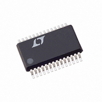
LTC1418IG Linear Technology, LTC1418IG Datasheet - Page 17

LTC1418IG
Manufacturer Part Number
LTC1418IG
Description
IC A/D CONV 14BIT SRL&PAR 28SSOP
Manufacturer
Linear Technology
Datasheet
1.LTC1418ACGPBF.pdf
(28 pages)
Specifications of LTC1418IG
Number Of Bits
14
Sampling Rate (per Second)
200k
Data Interface
Serial, Parallel
Number Of Converters
1
Power Dissipation (max)
21.5mW Unipolar; 31.5mW Bipolar
Voltage Supply Source
Dual ±
Operating Temperature
-40°C ~ 85°C
Mounting Type
Surface Mount
Package / Case
28-SSOP (0.200", 5.30mm Width)
Lead Free Status / RoHS Status
Contains lead / RoHS non-compliant
Available stocks
Company
Part Number
Manufacturer
Quantity
Price
Company:
Part Number:
LTC1418IG
Manufacturer:
LT
Quantity:
2 027
Bypass capacitors must be located as close to the pins as
possible. The traces connecting the pins and the bypass
capacitors must be kept short and should be made as wide
as possible.
Example Layout
Figures 12a, 12b, 12c and 12d show the schematic and
layout of a suggested evaluation board. The layout demon-
strates the proper use of decoupling capacitors and ground
plane with a 2-layer printed circuit board.
DIGITAL INTERFACE
The LTC1418 can operate in serial or parallel mode. In
parallel mode the ADC is designed to interface with micro-
processors as a memory mapped device. The CS and RD
control inputs are common to all peripheral memory
interfacing. In serial mode only four digital interface lines
are required, SCLK, CONVST, EXTCLKIN and D
the serial data shift clock can be an external input or
supplied by the LTC1418 internal clock.
APPLICATIONS
U
INFORMATION
U
Figure 12d. Suggested Evaluation Circuit Board—Solder Side Layout
W
OUT
U
. SCLK,
Internal Clock
The ADC has an internal clock. In parallel output mode the
internal clock is always used as the conversion clock. In
serial output mode either the internal clock or an external
clock may be used as the conversion clock (see Figure 20).
The internal clock is factory trimmed to achieve a typical
conversion time of 3.4 s and a maximum conversion time
over the full operating temperature range of 4 s. No exter-
nal adjustments are required, and with the guaranteed maxi-
mum acquisition time of 1 s, throughput performance of
200ksps is assured.
Power Shutdown
The LTC1418 provides two power shutdown modes, nap
and sleep, to save power during inactive periods. The nap
mode reduces the power by 80% and leaves only the
digital logic and reference powered up. The wake-up time
from nap to active is 500ns (see Figure 13a). In sleep
mode all bias currents are shut down and only leakage
current remains— about 2 A. Wake-up time from sleep
1418 F12d
LTC1418
17


