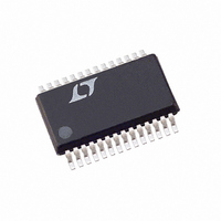
LTC1418IG Linear Technology, LTC1418IG Datasheet - Page 20

LTC1418IG
Manufacturer Part Number
LTC1418IG
Description
IC A/D CONV 14BIT SRL&PAR 28SSOP
Manufacturer
Linear Technology
Datasheet
1.LTC1418ACGPBF.pdf
(28 pages)
Specifications of LTC1418IG
Number Of Bits
14
Sampling Rate (per Second)
200k
Data Interface
Serial, Parallel
Number Of Converters
1
Power Dissipation (max)
21.5mW Unipolar; 31.5mW Bipolar
Voltage Supply Source
Dual ±
Operating Temperature
-40°C ~ 85°C
Mounting Type
Surface Mount
Package / Case
28-SSOP (0.200", 5.30mm Width)
Lead Free Status / RoHS Status
Contains lead / RoHS non-compliant
Available stocks
Company
Part Number
Manufacturer
Quantity
Price
Company:
Part Number:
LTC1418IG
Manufacturer:
LT
Quantity:
2 027
LTC1418
outputs; BUSY goes high releasing the processor and the
processor takes RD (= CONVST) back high and reads the
new conversion data.
In ROM mode, the processor takes RD (= CONVST) low,
starting a conversion and reading the previous conversion
result. After the conversion is complete, the processor can
read the new result and initiate another conversion.
Serial Output Mode
Serial output mode is selected when the SER/PAR input
pin is high. In this mode, Pins 16 to 20, D0 (EXT/INT), D1
(D
assume their serial functions as shown in Figure 20.
(During this discussion these pins will be referred to by
their serial function names: EXT/INT, D
SCLK and EXTCLKIN.) As in parallel mode, conversions
are started by a falling CONVST edge with CS low. After a
conversion is completed and the output shift register has
been updated, BUSY will go high and valid data will be
available on D
20
APPLICATIONS
OUT
), D2 (CLKOUT), D3 (SCLK) and D4 (EXTCLKIN)
RD = CONVST
OUT
RD = CONVST
CS = 0
BUSY
DATA
(Pin 19). This data can be clocked out
U
CS = 0
BUSY
DATA
INFORMATION
U
(SAMPLE N)
t
6
t
10
(SAMPLE N)
t
6
t
W
10
DB13 TO DB0
DATA (N – 1)
t
CONV
DB13 TO DB0
DATA (N – 1)
Figure 18. Slow Memory Mode Timing
OUT
t
CONV
, CLKOUT,
t
Figure 19. ROM Mode Timing
11
U
t
7
DB13 TO DB0
DATA N
t
11
t
8
either before the next conversion starts or it can be clocked
out during the next conversion. To enable the serial data
output buffer and shift clock, CS and RD must be low.
Figure 20 shows a function block diagram of the LTC1418
in serial mode. There are two pieces to this circuitry: the
conversion clock selection circuit (EXT/INT, EXTCLKIN
and CLKOUT) and the serial port (SCLK, D
Conversion Clock Selection (Serial Mode)
In Figure 20, the conversion clock controls the internal
ADC operation. The conversion clock can be either inter-
nal or external. By connecting EXT/INT low, the internal
clock is selected. This clock generates 16 clock cycles
which feed into the SAR for each conversion.
To select an external conversion clock, tie EXT/INT high
and apply an external conversion clock to EXTCLKIN (Pin
16). (When an external shift clock (SCLK) is used during
a conversion, the SCLK should be used as the external
conversion clock to avoid the noise generated by the
t
8
DB13 TO DB0
DATA N
DB13 TO DB0
DATA N
DB13 TO DB0
DATA (N + 1)
1418 F18
1418 F19
OUT
, CS and RD).


