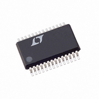
LTC1418IG Linear Technology, LTC1418IG Datasheet - Page 8

LTC1418IG
Manufacturer Part Number
LTC1418IG
Description
IC A/D CONV 14BIT SRL&PAR 28SSOP
Manufacturer
Linear Technology
Datasheet
1.LTC1418ACGPBF.pdf
(28 pages)
Specifications of LTC1418IG
Number Of Bits
14
Sampling Rate (per Second)
200k
Data Interface
Serial, Parallel
Number Of Converters
1
Power Dissipation (max)
21.5mW Unipolar; 31.5mW Bipolar
Voltage Supply Source
Dual ±
Operating Temperature
-40°C ~ 85°C
Mounting Type
Surface Mount
Package / Case
28-SSOP (0.200", 5.30mm Width)
Lead Free Status / RoHS Status
Contains lead / RoHS non-compliant
Available stocks
Company
Part Number
Manufacturer
Quantity
Price
Company:
Part Number:
LTC1418IG
Manufacturer:
LT
Quantity:
2 027
FUNCTIONAL BLOCK DIAGRA
APPLICATIONS
LTC1418
CONVERSION DETAILS
The LTC1418 uses a successive approximation algorithm
and an internal sample-and-hold circuit to convert an
analog signal to a 14-bit parallel or serial output. The ADC
is complete with a precision reference and an internal
clock. The control logic provides easy interface to micro-
processors and DSPs (please refer to Digital Interface
section for the data format).
Conversion start is controlled by the CS and CONVST
inputs. At the start of the conversion the successive
approximation register (SAR) is reset. Once a conversion
cycle has begun it cannot be restarted.
During the conversion, the internal differential 14-bit
capacitive DAC output is sequenced by the SAR from the
most significant bit (MSB) to the least significant bit (LSB).
8
REFCOMP
DGND
AGND
U
V
A
A
REF
IN
IN
+
–
NOTE: PIN NAMES IN PARENTHESES
2.5V
4.096V
U
INTERNAL
REFER TO SERIAL MODE
CLOCK
8k
D4 (EXTCLKIN)
U
REF AMP
2.5V REF
INFORMATION
U
D0 (EXT/INT)
MUX
W
SHDN
SUCCESSIVE APPROXIMATION
14-BIT CAPACITIVE DAC
CONVST RD CS
C
C
CONTROL LOGIC
SAMPLE
SAMPLE
U
W
REGISTER
SER/PAR
A
A
D2/(CLKOUT)
IN
IN
+
–
SAMPLE
SAMPLE
ZEROING SWITCHES
BUSY
+
–
Figure 1. Simplified Block Diagram
V
COMP
DAC
14
+
V
HOLD
HOLD
DAC
REGISTER
–
SHIFT
C
C
SAMPLE
SAMPLE
C
C
DAC
DAC
+
–
+
–
SAR
1418 BD
ZEROING SWITCHES
•
•
•
+
–
14
D13
D0
D3/(SCLK)
V
V
D1/(D
COMP
HOLD
HOLD
DD
SS
: 0V FOR UNIPOLAR MODE
: 5V
– 5V FOR BIPOLAR MODE
OUT
OUTPUT
LATCH
)
1418 F01
D13
D0


