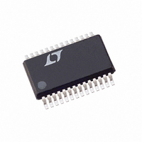
LTC1418IG Linear Technology, LTC1418IG Datasheet - Page 21

LTC1418IG
Manufacturer Part Number
LTC1418IG
Description
IC A/D CONV 14BIT SRL&PAR 28SSOP
Manufacturer
Linear Technology
Datasheet
1.LTC1418ACGPBF.pdf
(28 pages)
Specifications of LTC1418IG
Number Of Bits
14
Sampling Rate (per Second)
200k
Data Interface
Serial, Parallel
Number Of Converters
1
Power Dissipation (max)
21.5mW Unipolar; 31.5mW Bipolar
Voltage Supply Source
Dual ±
Operating Temperature
-40°C ~ 85°C
Mounting Type
Surface Mount
Package / Case
28-SSOP (0.200", 5.30mm Width)
Lead Free Status / RoHS Status
Contains lead / RoHS non-compliant
Available stocks
Company
Part Number
Manufacturer
Quantity
Price
Company:
Part Number:
LTC1418IG
Manufacturer:
LT
Quantity:
2 027
APPLICATIONS
asynchronous clocks. To maintain accuracy the external
conversion clock frequency must be between 30kHz and
4.5MHz.) The SAR sends an end of conversion signal,
EOC, that gates the external conversion clock so that only
16 clock cycles can go into the SAR, even if the external
clock, EXTCLKIN, contains more than 16 cycles.
When CS and RD are low, these 16 cycles of conversion
clock (whether internally or externally generated) will
appear on CLKOUT during each conversion and then
CLKOUT will remain low until the next conversion. If
desired, CLKOUT can be used as a master clock to drive
the serial port. Because CLKOUT is running during the
conversion, it is important to avoid excessive loading that
can cause large supply transients and create noise. For
the best performance, limit CLKOUT loading to 20pF.
Serial Port
The serial port in Figure 20 is made up of a 16-bit shift
register and a three-state output buffer that are con-
trolled by three inputs: SCLK, RD and CS. The serial port
has one output, D
data.
SAR
U
OUT
, that provides the serial output
INFORMATION
U
DATA
Figure 20. Functional Block Diagram for Serial Mode (SER/PAR = High)
EOC
IN
14
16 CONVERSION CLOCK CYCLES
CLOCK
INPUT
W
REGISTER
SHIFT
U
DATA
OUT
*PINS 16 TO 20 ARE LABELED WITH THEIR SERIAL FUNCTIONS
BUFFER
THREE
STATE
INTERNAL
CLOCK
The SCLK is used to clock the shift register. Data may be
clocked out with the internal conversion clock operating
as a master by connecting CLKOUT (Pin 18) to SCLK (Pin
17) or with an external data clock applied to D3 (SCLK).
The minimum number of SCLK cycles required to
transfer a data word is 14. Normally, SCLK contains 16
clock cycles for a word length of 16 bits; 14 bits with MSB
first, followed by two trailing zeros.
A logic high on RD disables SCLK and three-states D
In case of using a continuous SCLK, RD can be controlled
to limit the number of shift clocks to the desired number
(i.e., 16 cycles) and to three-state D
transfer.
A logic high on CS three-states the D
also inhibits conversion when it is tied high. In power
shutdown mode (SHDN = low), a high CS selects sleep
mode while a low CS selects nap mode. For normal serial
port operation, CS can be grounded.
D
falling edge of each SCLK (see Figures 21 and 22). If 16
SCLKs are provided, the 14 data bits will be followed by
BUFFER
THREE
STATE
OUT
outputs the serial data; 14 bits, MSB first, on the
• • •
• • •
17
23
25
19
18
16
20
26
SCLK*
RD
CS
D
CLKOUT*
EXTCLKIN*
EXT/INT*
BUSY
1418 F20
OUT
OUT
*
OUT
output buffer. It
LTC1418
after the data
21
OUT
.


