HI5628INZ Intersil, HI5628INZ Datasheet - Page 10
HI5628INZ
Manufacturer Part Number
HI5628INZ
Description
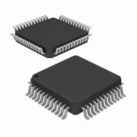
IC DAC 8BIT 125MSPS DUAL 48-LQFP
Manufacturer
Intersil
Datasheet
1.HI56286IN.pdf
(10 pages)
Specifications of HI5628INZ
Number Of Bits
8
Data Interface
Parallel
Number Of Converters
2
Voltage Supply Source
Analog and Digital
Power Dissipation (max)
330mW
Operating Temperature
-40°C ~ 85°C
Mounting Type
Surface Mount
Package / Case
48-LQFP
Lead Free Status / RoHS Status
Lead free / RoHS Compliant
Settling Time
-
Available stocks
Company
Part Number
Manufacturer
Quantity
Price


Pin Descriptions
Intersil products are sold by description only. Intersil Corporation reserves the right to make changes in circuit design, software and/or specifications at any time without
notice. Accordingly, the reader is cautioned to verify that data sheets are current before placing orders. Information furnished by Intersil is believed to be accurate and
reliable. However, no responsibility is assumed by Intersil or its subsidiaries for its use; nor for any infringements of patents or other rights of third parties which may result
from its use. No license is granted by implication or otherwise under any patent or patent rights of Intersil or its subsidiaries.
6, 7, 10, 28, 30,
13, 18, 19, 25
9, 29, 40, 45
1-5, 48-46
31, 41, 44
PIN NO.
14, 24
11, 27
12, 26
39-32
15
23
22
17
16
20
21
43
42
8
All Intersil U.S. products are manufactured, assembled and tested utilizing ISO9000 quality systems.
QD7 (MSB) Through
ID7 (MSB) Through
ICOMP1, QCOMP1
Intersil Corporation’s quality certifications can be viewed at www.intersil.com/design/quality
PIN NAME
QD0 (LSB)
ID0 (LSB)
QOUTB
QOUTA
REFLO
SLEEP
FSADJ
For information regarding Intersil Corporation and its products, see www.intersil.com
REFIO
IOUTB
AGND
IOUTA
DGND
DV
QCLK
AV
ICLK
NC
DD
DD
10
Digital Data Bit 7, the Most Significant Bit through Digital Data Bit 0, the Least Significant Bit, of the Q
channel.
Digital Data Bit 7, the Most Significant Bit through Digital Data Bit 0, the Least Significant Bit, of the I
channel.
Control Pin for Power-Down Mode. Sleep Mode is active high; connect to ground for Normal Mode. Sleep
pin has internal 20µA active pulldown current.
Connect to analog ground to enable internal 1.2V reference or connect to AV
Reference voltage input if internal reference is disabled and reference voltage output if internal reference is
enabled. Use 0.1µF cap to ground when internal reference is enabled.
Full Scale Current Adjust. Use a resistor to ground to adjust full scale output current. Full Scale Output
Current Per Channel = 32 x I
Reduces noise. Connect each to AV
tied together externally.
Analog Ground Connections.
The complementary current output of the I channel. Bits set to all 0s gives full scale current.
Current output of the I channel. Bits set to all 1s gives full scale current.
The complementary current output of the Q channel. Bits set to all 0s gives full scale current.
Current output of the Q channel. Bits set to all 1s gives full scale current.
No Connect. Recommended: Connect to ground.
Analog Supply (+2.7V to +5.5V).
Digital Ground.
Supply voltage for digital circuitry (+2.7V to +5.5V).
Clock input for I channel. Positive edge of clock latches data.
Clock input for Q channel. Positive edge of clock latches data.
HI5628
FSADJ
.
DD
with 0.1µF capacitor. The ICOMP1 and QCOMP1 pins MUST be
PIN DESCRIPTION
DD
to disable.
Related parts for HI5628INZ
Image
Part Number
Description
Manufacturer
Datasheet
Request
R

Part Number:
Description:
DAC DUAL 8BIT 60MSPS 48LQFP
Manufacturer:
Intersil
Datasheet:
Part Number:
Description:
IC DAC 8BIT 60MSPS DUAL 48-LQFP
Manufacturer:
Intersil
Datasheet:

Part Number:
Description:
8-Bit, 165/125/60MSPS, Dual High Speed CMOS D/A Converter
Manufacturer:
INTERSIL [Intersil Corporation]
Datasheet:
Part Number:
Description:
DAC DUAL 8BIT 60MSPS 48LQFP
Manufacturer:
Intersil
Datasheet:

Part Number:
Description:
8-bit, 165/125/60 Msps, Dual High Speed Cmos D/a Converter
Manufacturer:
Intersil Corporation
Datasheet:
Part Number:
Description:
Intersil Corporation [CMOS Serial Controller Interface]
Manufacturer:
Intersil Corporation
Datasheet:
Part Number:
Description:
Manufacturer:
Intersil Corporation
Datasheet:
Part Number:
Description:
357-036-542-201 CARDEDGE 36POS DL .156 BLK LOPRO
Manufacturer:
Intersil Corporation
Datasheet:
Part Number:
Description:
1024-Word x 4-Bit LSI Static RAM
Manufacturer:
Intersil Corporation
Datasheet:
Part Number:
Description:
General Purpose NPN Transistor Arrays FN341.4
Manufacturer:
Intersil Corporation
Datasheet:
Part Number:
Description:
CMOS 16-Bit Microprocessor
Manufacturer:
Intersil Corporation
Datasheet:
Part Number:
Description:
Manufacturer:
Intersil Corporation
Datasheet:
Part Number:
Description:
Manufacturer:
Intersil Corporation
Datasheet:
Part Number:
Description:
Manufacturer:
Intersil Corporation
Datasheet:
Part Number:
Description:
Manufacturer:
Intersil Corporation
Datasheet: