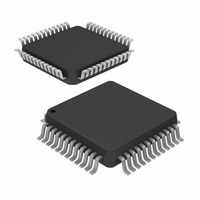
HI5628INZ Intersil, HI5628INZ Datasheet - Page 4

HI5628INZ
Manufacturer Part Number
HI5628INZ
Description
IC DAC 8BIT 125MSPS DUAL 48-LQFP
Manufacturer
Intersil
Datasheet
1.HI56286IN.pdf
(10 pages)
Specifications of HI5628INZ
Number Of Bits
8
Data Interface
Parallel
Number Of Converters
2
Voltage Supply Source
Analog and Digital
Power Dissipation (max)
330mW
Operating Temperature
-40°C ~ 85°C
Mounting Type
Surface Mount
Package / Case
48-LQFP
Lead Free Status / RoHS Status
Lead free / RoHS Compliant
Settling Time
-
Available stocks
Company
Part Number
Manufacturer
Quantity
Price
Absolute Maximum Ratings
Digital Supply Voltage DV
Analog Supply Voltage AV
Grounds, ACOM TO DCOM . . . . . . . . . . . . . . . . . . . -0.3V to +0.3V
Digital Input Voltages (D7-D0, CLK, SLEEP). . . . . . . . DV
Internal Reference Output Current. . . . . . . . . . . . . . . . . . . . . ±50µA
Reference Input Voltage Range . . . . . . . . . . . . . . . . . . AV
Analog Output Current (I
Operating Conditions
Temperature Range . . . . . . . . . . . . . . . . . . . . . . . . . . -40
CAUTION: Stresses above those listed in “Absolute Maximum Ratings” may cause permanent damage to the device. This is a stress only rating and operation of the
device at these or any other conditions above those indicated in the operational sections of this specification is not implied.
NOTE:
Electrical Specifications
SYSTEM PERFORMANCE (Per Channel)
Resolution
Integral Linearity Error, INL
Differential Linearity Error, DNL
Offset Error, I
Offset Drift Coefficient
Full Scale Gain Error, FSE
Full Scale Gain Drifta
Gain Matching Between Channels
I/Q Channel Isolation
Output Voltage Compliance Range
Full Scale Output Current, I
DYNAMIC CHARACTERISTICS (Per Channel)
Clock Rate, f
Output Settling Time, (t
Singlet Glitch Area (Peak Glitch)
Output Rise Time
Output Fall Time
Output Capacitance
Output Noise
1. θ
JA
is measured with the component mounted on an evaluation PC board in free air.
CLK
OS
PARAMETER
SETT
OUT
DD
DD
FS
) . . . . . . . . . . . . . . . . . . . . . . . . . 24mA
to DCOM . . . . . . . . . . . . . . . . . . +5.5V
)
to ACOM . . . . . . . . . . . . . . . . . . +5.5V
4
AV
is per channel except for ‘Power Supply Characteristics.’
DD
= +5V , DV
“Best Fit” Straight Line (Note 7)
(Note 7)
(Note 7)
(Note 7)
With External Reference (Notes 2, 7)
With Internal Reference (Notes 2, 7)
With External Reference (Note 7)
With Internal Reference (Note 7)
F
(Note 3)
(Note 3, 9)
0.8% (±1 LSB, equivalent to 7 Bits) (Note 7)
0.4% (±1/2 LSB, equivalent to 8 Bits) (Note 7)
R
Full Scale Step
Full Scale Step
IOUTFS = 20mA
IOUTFS = 2mA
OUT
L
= 25Ω (Note 7)
= 10MHz
DD
= +5V, V
o
DD
DD
C to 85
+ 0.3V
+ 0.3V
REF
o
C
TEST CONDITIONS
HI5628
= Internal 1.2V, IOUTFS = 20mA, T
Thermal Information
Thermal Resistance (Typical, Note 1)
Maximum Junction Temperature . . . . . . . . . . . . . . . . . . . . . . .150
Maximum Storage Temperature Range . . . . . . . . . . -65
Maximum Lead Temperature (Soldering 10s) . . . . . . . . . . . . .300
LQFP Package . . . . . . . . . . . . . . . . . . . . . . . . . . . . .
A
= 25
o
C for All Typical Values. Data given
-0.025
MIN
T
-0.5
-0.5
-0.5
-0.3
125
-10
-10
A
8
2
-
-
-
-
-
-
-
-
-
-
-
-
= -40
HI5628IN
±0.25
±0.25
±100
TYP
o
±50
0.1
0.1
1.5
1.5
±2
±1
80
15
10
50
30
C TO 85
5
5
-
-
-
-
-
+0.025
MAX
+0.5
+0.5
1.25
+10
+10
0.5
20
o
-
-
-
-
-
-
-
-
-
-
-
-
-
-
C
o
θ
C to 150
JA
% FSR
% FSR
% FSR
UNITS
FSR/
FSR/
FSR/
pA/ √Hz
pA/ √Hz
(
MHz
pV•s
75
LSB
LSB
Bits
ppm
ppm
ppm
o
mA
dB
dB
pF
ns
ns
ns
ns
C/W)
V
o
o
o
C
C
C
o
o
o
C
C
C


