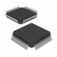
HI5628INZ Intersil, HI5628INZ Datasheet - Page 8

HI5628INZ
Manufacturer Part Number
HI5628INZ
Description
IC DAC 8BIT 125MSPS DUAL 48-LQFP
Manufacturer
Intersil
Datasheet
1.HI56286IN.pdf
(10 pages)
Specifications of HI5628INZ
Number Of Bits
8
Data Interface
Parallel
Number Of Converters
2
Voltage Supply Source
Analog and Digital
Power Dissipation (max)
330mW
Operating Temperature
-40°C ~ 85°C
Mounting Type
Surface Mount
Package / Case
48-LQFP
Lead Free Status / RoHS Status
Lead free / RoHS Compliant
Settling Time
-
Available stocks
Company
Part Number
Manufacturer
Quantity
Price
Definition of Specifications
Integral Linearity Error, INL, is the measure of the worst
case point that deviates from a best fit straight line of data
values along the transfer curve.
Differential Linearity Error, DNL, is the measure of the
step size output deviation from code to code. Ideally the step
size should be 1 LSB. A DNL specification of 1 LSB or less
guarantees monotonicity.
Output Settling Time, is the time required for the output
voltage to settle to within a specified error band measured
from the beginning of the output transition. The
measurement was done by switching from code 0 to 64, or
quarter scale. Termination impedance was 25
parallel resistance of the output 50
50
error band without overdriving the oscilloscope.
Singlet Glitch Area, is the switching transient appearing on
the output during a code transition. It is measured as the
area under the overshoot portion of the curve and is
expressed as a Volt-Time specification.
Full Scale Gain Error , is the error from an ideal ratio of 32
between the output current and the full scale adjust current
(through R
Full Scale Gain Drift, is measured by setting the data inputs
to all ones and measuring the output voltage through a
known resistance as the temperature is varied from T
T
measured at room temperature to the value measured at
either T
Range) per degree C.
Total Harmonic Distortion, THD, is the ratio of the DAC output
fundamental to the RMS sum of the first five harmonics.
Spurious Free Dynamic Range, SFDR, is the amplitude
difference from the fundamental to the largest harmonically
or non-harmonically related spur within the specified
window.
Output Voltage Compliance Range, is the voltage limit
imposed on the output. The output impedance load should
be chosen such that the voltage developed does not violate
the compliance range.
Offset Error, is measured by setting the data inputs to all
zeros and measuring the output voltage through a known
resistance. Offset error is defined as the maximum deviation
of the output current from a value of 0mA.
Offset Drift, is measured by setting the data inputs to all
zeros and measuring the output voltage through a known
resistance as the temperature is varied from T
It is defined as the maximum deviation from the value
measured at room temperature to the value measured at
MAX
Ω
input. This also aids the ability to resolve the specified
. It is defined as the maximum deviation from the value
MIN
SET
or T
).
MAX
. The units are ppm of FSR (Full Scale
8
Ω
and the oscilloscope’s
Ω
MIN
due to the
to T
MIN
MAX
to
.
HI5628
either T
Range) per degree C.
Power Supply Rejection, is measured using a single power
supply. Its nominal +5V is varied
DAC full scale output is noted.
Reference Input Multiplying Bandwidth, is defined as the
3dB bandwidth of the voltage reference input. It is measured
by using a sinusoidal waveform as the external reference
with the digital inputs set to all 1s. The frequency is
increased until the amplitude of the output waveform is
0.707 of its original value.
Internal Reference Voltage Drift, is defined as the
maximum deviation from the value measured at room
temperature to the value measured at either T
The units are ppm per degree C.
Detailed Description
The HI5628 is a dual, 8-bit, current out, CMOS, digital to
analog converter. Its maximum update rate is 125MSPS and
can be powered by either single or dual power supplies in
the recommended range of +3V to +5V. It consumes less
than 330mW of power when using a +5V supply with the
data switching at 100MSPS. The architecture is based on a
segmented current source arrangement that reduces glitch
by reducing the amount of current switching at any one time.
The five MSBs are represented by 31 major current sources
of equivalent current. The three LSBs are comprised of
binary weighted current sources. Consider an input pattern
to the converter which ramps through all the codes from 0 to
255. The three LSB current sources would begin to count up.
When they reached the all high state (decimal value of 7)
and needed to count to the next code, they would all turn off
and the first major current source would turn on. To continue
counting upward, the 3 LSBs would count up another 7
codes, and then the next major current source would turn on
and the three LSBs would all turn off. The process of the
single, equivalent, major current source turning on and the
three LSBs turning off each time the converter reaches
another 7 codes greatly reduces the glitch at any one
switching point. In previous architectures that contained all
binary weighted current sources or a binary weighted
resistor ladder, the converter might have a substantially
larger amount of current turning on and off at certain, worst-
case transition points such as midscale and quarter scale
transitions. By greatly reducing the amount of current
switching at certain ‘major’ transitions, the overall glitch of
the converter is dramatically reduced, improving settling
times and transient problems.
MIN
or T
MAX
. The units are ppm of FSR (Full Scale
±
10% and the change in the
MIN
or T
MAX
.


