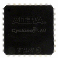
EP3C10E144C8N Altera, EP3C10E144C8N Datasheet - Page 109

EP3C10E144C8N
Manufacturer Part Number
EP3C10E144C8N
Description
IC CYCLONE III FPGA 10K 144-EQFP
Manufacturer
Altera
Series
Cyclone® IIIr
Datasheets
1.EP3C5F256C8N.pdf
(5 pages)
2.EP3C5F256C8N.pdf
(34 pages)
3.EP3C5F256C8N.pdf
(66 pages)
4.EP3C5F256C8N.pdf
(14 pages)
5.EP3C5F256C8N.pdf
(76 pages)
6.EP3C10E144C8N.pdf
(274 pages)
Specifications of EP3C10E144C8N
Number Of Logic Elements/cells
10320
Number Of Labs/clbs
645
Total Ram Bits
423936
Number Of I /o
94
Voltage - Supply
1.15 V ~ 1.25 V
Mounting Type
Surface Mount
Operating Temperature
0°C ~ 85°C
Package / Case
144-EQFP
Family Name
Cyclone III
Number Of Logic Blocks/elements
10320
# I/os (max)
94
Frequency (max)
402MHz
Process Technology
65nm
Operating Supply Voltage (typ)
1.2V
Logic Cells
10320
Ram Bits
423936
Operating Supply Voltage (min)
1.15V
Operating Supply Voltage (max)
1.25V
Operating Temp Range
0C to 85C
Operating Temperature Classification
Commercial
Mounting
Surface Mount
Pin Count
144
Package Type
EQFP
For Use With
544-2601 - KIT DEV CYCLONE III LS EP3CLS200544-2411 - KIT DEV NIOS II CYCLONE III ED.
Lead Free Status / RoHS Status
Lead free / RoHS Compliant
Number Of Gates
-
Lead Free Status / Rohs Status
Compliant
Other names
544-2427
EP3C10E144C8N
EP3C10E144C8N
Available stocks
Company
Part Number
Manufacturer
Quantity
Price
Company:
Part Number:
EP3C10E144C8N
Manufacturer:
ALTERA47
Quantity:
516
Part Number:
EP3C10E144C8N
Manufacturer:
ALTERA
Quantity:
20 000
Chapter 6: I/O Features in the Cyclone III Device Family
OCT Support
© December 2009
Altera Corporation
Figure 6–3
Figure 6–3. Cyclone III Device Family OCT Block Placement
Each calibration block comes with a pair of RUP and RDN pins. When used for
calibration, the RUP pin is connected to V
50-Ω ±1% resistor for an on-chip series termination value of 25 Ω or 50 Ω,
respectively. The RDN pin is connected to GND through an external 25-Ω ±1% or 50-Ω
The external resistors are compared with the internal resistance using comparators.
The resultant outputs of the comparators are used by the OCT calibration block to
dynamically adjust buffer impedance.
During calibration, the resistance of the RUP and RDN pins varies. For an estimate of
the maximum possible current through the external calibration resistors, assume a
minimum resistance of 0 Ω on the RUP and RDN pins during calibration.
±1% resistor for an on-chip series termination value of 25 Ω or 50 Ω, respectively.
shows the top-level view of the OCT calibration blocks placement.
I/O Bank 3
I/O Bank 8
Cyclone III Device Family
I/O Bank 4
I/O Bank 7
CCIO
through an external 25-Ω ±1% or
Cyclone III Device Handbook, Volume 1
I/O bank with
calibration block
I/O bank without
calibration block
Calibration block
coverage
6–9


