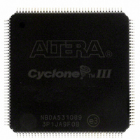
EP3C10E144C8N Altera, EP3C10E144C8N Datasheet - Page 272

EP3C10E144C8N
Manufacturer Part Number
EP3C10E144C8N
Description
IC CYCLONE III FPGA 10K 144-EQFP
Manufacturer
Altera
Series
Cyclone® IIIr
Datasheets
1.EP3C5F256C8N.pdf
(5 pages)
2.EP3C5F256C8N.pdf
(34 pages)
3.EP3C5F256C8N.pdf
(66 pages)
4.EP3C5F256C8N.pdf
(14 pages)
5.EP3C5F256C8N.pdf
(76 pages)
6.EP3C10E144C8N.pdf
(274 pages)
Specifications of EP3C10E144C8N
Number Of Logic Elements/cells
10320
Number Of Labs/clbs
645
Total Ram Bits
423936
Number Of I /o
94
Voltage - Supply
1.15 V ~ 1.25 V
Mounting Type
Surface Mount
Operating Temperature
0°C ~ 85°C
Package / Case
144-EQFP
Family Name
Cyclone III
Number Of Logic Blocks/elements
10320
# I/os (max)
94
Frequency (max)
402MHz
Process Technology
65nm
Operating Supply Voltage (typ)
1.2V
Logic Cells
10320
Ram Bits
423936
Operating Supply Voltage (min)
1.15V
Operating Supply Voltage (max)
1.25V
Operating Temp Range
0C to 85C
Operating Temperature Classification
Commercial
Mounting
Surface Mount
Pin Count
144
Package Type
EQFP
For Use With
544-2601 - KIT DEV CYCLONE III LS EP3CLS200544-2411 - KIT DEV NIOS II CYCLONE III ED.
Lead Free Status / RoHS Status
Lead free / RoHS Compliant
Number Of Gates
-
Lead Free Status / Rohs Status
Compliant
Other names
544-2427
EP3C10E144C8N
EP3C10E144C8N
Available stocks
Company
Part Number
Manufacturer
Quantity
Price
Company:
Part Number:
EP3C10E144C8N
Manufacturer:
ALTERA47
Quantity:
516
Part Number:
EP3C10E144C8N
Manufacturer:
ALTERA
Quantity:
20 000
12–6
Guidelines for IEEE Std. 1149.1 BST
Cyclone III Device Handbook, Volume 1
Figure 12–1
inserted in the chain.
Figure 12–1. JTAG Chain of Mixed Voltages
Use the following guidelines when performing BST with IEEE Std. 1149.1 devices:
■
■
■
■
If the 10 bit checkerboard pattern (1010101010) does not shift out of the instruction
register via the TDO pin during the first clock cycle of the SHIFT_IR state, the TAP
controller did not reach the proper state. To solve this problem, try one of the
following procedures:
■
■
Perform a SAMPLE/PRELOAD test cycle prior to the first EXTEST test cycle to
ensure that known data is present at the device pins when you enter the EXTEST
mode. If the OEJ update register contains a 0, the data in the OUTJ update register
is driven out. The state must be known and correct to avoid contention with other
devices in the system.
Do not perform EXTEST testing during ICR. This instruction is supported before
or after ICR, but not during ICR. Use the CONFIG_IO instruction to interrupt
configuration and then perform testing, or wait for configuration to complete.
If testing is performed before configuration, hold the nCONFIG pin low.
Verify that the TAP controller has reached the SHIFT_IR state correctly. To
advance the TAP controller to the SHIFT_IR state, return to the RESET state
and send the code 01100 to the TMS pin.
Check the connections to the VCC, GND, JTAG, and dedicated configuration
pins on the device.
shows the JTAG chain of mixed voltages and how a level shifter is
Tester
TDO
TDI
tester if necessary
level accepted by
Shift TDO to
Shifter
Chapter 12: IEEE 1149.1 (JTAG) Boundary-Scan Testing for the Cyclone III Device Family
Level
V
3.3 V
CCIO
Must be
tolerant
V
1.5 V
1.8 V
CCIO
Must be
tolerant
V
2.5 V
3.3 V
CCIO
© December 2009 Altera Corporation
Guidelines for IEEE Std. 1149.1 BST
Must be
tolerant
V
1.8 V
2.5 V
CCIO


