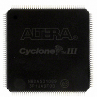
EP3C10E144C8N Altera, EP3C10E144C8N Datasheet - Page 49

EP3C10E144C8N
Manufacturer Part Number
EP3C10E144C8N
Description
IC CYCLONE III FPGA 10K 144-EQFP
Manufacturer
Altera
Series
Cyclone® IIIr
Datasheets
1.EP3C5F256C8N.pdf
(5 pages)
2.EP3C5F256C8N.pdf
(34 pages)
3.EP3C5F256C8N.pdf
(66 pages)
4.EP3C5F256C8N.pdf
(14 pages)
5.EP3C5F256C8N.pdf
(76 pages)
6.EP3C10E144C8N.pdf
(274 pages)
Specifications of EP3C10E144C8N
Number Of Logic Elements/cells
10320
Number Of Labs/clbs
645
Total Ram Bits
423936
Number Of I /o
94
Voltage - Supply
1.15 V ~ 1.25 V
Mounting Type
Surface Mount
Operating Temperature
0°C ~ 85°C
Package / Case
144-EQFP
Family Name
Cyclone III
Number Of Logic Blocks/elements
10320
# I/os (max)
94
Frequency (max)
402MHz
Process Technology
65nm
Operating Supply Voltage (typ)
1.2V
Logic Cells
10320
Ram Bits
423936
Operating Supply Voltage (min)
1.15V
Operating Supply Voltage (max)
1.25V
Operating Temp Range
0C to 85C
Operating Temperature Classification
Commercial
Mounting
Surface Mount
Pin Count
144
Package Type
EQFP
For Use With
544-2601 - KIT DEV CYCLONE III LS EP3CLS200544-2411 - KIT DEV NIOS II CYCLONE III ED.
Lead Free Status / RoHS Status
Lead free / RoHS Compliant
Number Of Gates
-
Lead Free Status / Rohs Status
Compliant
Other names
544-2427
EP3C10E144C8N
EP3C10E144C8N
Available stocks
Company
Part Number
Manufacturer
Quantity
Price
Company:
Part Number:
EP3C10E144C8N
Manufacturer:
ALTERA47
Quantity:
516
Part Number:
EP3C10E144C8N
Manufacturer:
ALTERA
Quantity:
20 000
Chapter 3: Memory Blocks in the Cyclone III Device Family
Memory Modes
Figure 3–12. Cyclone III Device Family True Dual-Port Timing Waveforms
Shift Register Mode
© December 2009
q_a (asynch)
q_b (asynch)
address_a
address_b
data_a
rden_a
wren_a
wren_b
rden_b
clk_a
clk_b
Altera Corporation
din-1
an-1
doutn-1
Figure 3–12
and read operation at port B. Registering the outputs of the RAM simply delays the q
outputs by one clock cycle.
Cyclone III device family M9K memory blocks can implement shift registers for
digital signal processing (DSP) applications, such as finite impulse response (FIR)
filters, pseudo-random number generators, multi-channel filtering, and
auto-correlation and cross-correlation functions. These and other DSP applications
require local data storage, traditionally implemented with standard flipflops that
quickly exhaust many logic cells for large shift registers. A more efficient alternative is
to use embedded memory as a shift register block, which saves logic cell and routing
resources.
The size of a (w × m × n) shift register is determined by the input data width (w), the
length of the taps (m), and the number of taps (n), and must be less than or equal to
the maximum number of memory bits, which is 9,216 bits. In addition, the size of
(w × n) must be less than or equal to the maximum width of the block, which is 36 bits.
If you need a larger shift register, you can cascade the M9K memory blocks.
bn
din-1
din
an
shows true dual-port timing waveforms for the write operation at port A
doutn
din
b0
a0
dout0
a1
dout0
dout1
b1
a2
dout2
a3
dout3
dout1
b2
din4
a4
Cyclone III Device Handbook, Volume 1
din4
din5
a5
dout2
din5
b3
din6
a6
3–13


