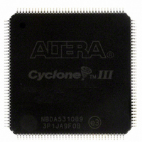
EP3C10E144C8N Altera, EP3C10E144C8N Datasheet - Page 42

EP3C10E144C8N
Manufacturer Part Number
EP3C10E144C8N
Description
IC CYCLONE III FPGA 10K 144-EQFP
Manufacturer
Altera
Series
Cyclone® IIIr
Datasheets
1.EP3C5F256C8N.pdf
(5 pages)
2.EP3C5F256C8N.pdf
(34 pages)
3.EP3C5F256C8N.pdf
(66 pages)
4.EP3C5F256C8N.pdf
(14 pages)
5.EP3C5F256C8N.pdf
(76 pages)
6.EP3C10E144C8N.pdf
(274 pages)
Specifications of EP3C10E144C8N
Number Of Logic Elements/cells
10320
Number Of Labs/clbs
645
Total Ram Bits
423936
Number Of I /o
94
Voltage - Supply
1.15 V ~ 1.25 V
Mounting Type
Surface Mount
Operating Temperature
0°C ~ 85°C
Package / Case
144-EQFP
Family Name
Cyclone III
Number Of Logic Blocks/elements
10320
# I/os (max)
94
Frequency (max)
402MHz
Process Technology
65nm
Operating Supply Voltage (typ)
1.2V
Logic Cells
10320
Ram Bits
423936
Operating Supply Voltage (min)
1.15V
Operating Supply Voltage (max)
1.25V
Operating Temp Range
0C to 85C
Operating Temperature Classification
Commercial
Mounting
Surface Mount
Pin Count
144
Package Type
EQFP
For Use With
544-2601 - KIT DEV CYCLONE III LS EP3CLS200544-2411 - KIT DEV NIOS II CYCLONE III ED.
Lead Free Status / RoHS Status
Lead free / RoHS Compliant
Number Of Gates
-
Lead Free Status / Rohs Status
Compliant
Other names
544-2427
EP3C10E144C8N
EP3C10E144C8N
Available stocks
Company
Part Number
Manufacturer
Quantity
Price
Company:
Part Number:
EP3C10E144C8N
Manufacturer:
ALTERA47
Quantity:
516
Part Number:
EP3C10E144C8N
Manufacturer:
ALTERA
Quantity:
20 000
3–6
Cyclone III Device Handbook, Volume 1
Figure 3–3
feeds back to its input using a multiplexer. The multiplexer output is selected by the
address clock enable (addressstall) signal.
Figure 3–3. Cyclone III Device Family Address Clock Enable Block Diagram
The address clock enable is typically used to improve the effectiveness of cache
memory applications during a cache-miss. The default value for the address clock
enable signals is low.
Figure 3–4
write cycles, respectively.
Figure 3–4. Cyclone III Device Family Address Clock Enable During Read Cycle Waveform
latched address
(inside memory)
addressstall
q (asynch)
rdaddress
q (synch)
inclock
shows an address clock enable block diagram. The address register output
and
rden
Figure 3–5
doutn-1
doutn
addressstall
an
address[N]
address[0]
a0
clock
doutn
show the address clock enable waveform during read and
a0
dout0
a1
dout0
dout1
a2
Chapter 3: Memory Blocks in the Cyclone III Device Family
address[N]
address[0]
register
register
dout1
a1
dout1
a3
dout1
dout1
© December 2009 Altera Corporation
address[0]
address[N]
a4
dout1
a4
dout4
a5
dout4
a5
dout5
Overview
a6


