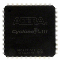
EP3C10E144C8N Altera, EP3C10E144C8N Datasheet - Page 210

EP3C10E144C8N
Manufacturer Part Number
EP3C10E144C8N
Description
IC CYCLONE III FPGA 10K 144-EQFP
Manufacturer
Altera
Series
Cyclone® IIIr
Datasheets
1.EP3C5F256C8N.pdf
(5 pages)
2.EP3C5F256C8N.pdf
(34 pages)
3.EP3C5F256C8N.pdf
(66 pages)
4.EP3C5F256C8N.pdf
(14 pages)
5.EP3C5F256C8N.pdf
(76 pages)
6.EP3C10E144C8N.pdf
(274 pages)
Specifications of EP3C10E144C8N
Number Of Logic Elements/cells
10320
Number Of Labs/clbs
645
Total Ram Bits
423936
Number Of I /o
94
Voltage - Supply
1.15 V ~ 1.25 V
Mounting Type
Surface Mount
Operating Temperature
0°C ~ 85°C
Package / Case
144-EQFP
Family Name
Cyclone III
Number Of Logic Blocks/elements
10320
# I/os (max)
94
Frequency (max)
402MHz
Process Technology
65nm
Operating Supply Voltage (typ)
1.2V
Logic Cells
10320
Ram Bits
423936
Operating Supply Voltage (min)
1.15V
Operating Supply Voltage (max)
1.25V
Operating Temp Range
0C to 85C
Operating Temperature Classification
Commercial
Mounting
Surface Mount
Pin Count
144
Package Type
EQFP
For Use With
544-2601 - KIT DEV CYCLONE III LS EP3CLS200544-2411 - KIT DEV NIOS II CYCLONE III ED.
Lead Free Status / RoHS Status
Lead free / RoHS Compliant
Number Of Gates
-
Lead Free Status / Rohs Status
Compliant
Other names
544-2427
EP3C10E144C8N
EP3C10E144C8N
Available stocks
Company
Part Number
Manufacturer
Quantity
Price
Company:
Part Number:
EP3C10E144C8N
Manufacturer:
ALTERA47
Quantity:
516
Part Number:
EP3C10E144C8N
Manufacturer:
ALTERA
Quantity:
20 000
9–50
Cyclone III Device Handbook, Volume 1
Figure 9–24. JTAG Configuration of a Single Device Using a Download Cable (2.5, 3.0, and 3.3-V
V
Notes to
(1) Connect these pull-up resistors to the V
(2) Connect the nCONFIG and MSEL[3..0] pins to support a non-JTAG configuration scheme. If you only use a JTAG
(3) Pin 6 of the header is a V
(4) The nCE pin must be connected to GND or driven low for successful JTAG configuration.
(5) The nCEO pin is left unconnected or used as a user I/O pin when it does not feed the nCE pin of another device.
(6) Power up the V
CCIO
configuration, connect the nCONFIG pin to logic high and the MSEL[3..0] pins to ground. In addition, pull DCLK
and DATA[0] either high or low, whichever is convenient on your board.
For this value, refer to the
ByteBlaster II, ByteBlasterMV, and Ethernet Blaster, this pin is a no connect.
from V
MasterBlaster cable. The MasterBlaster cable can receive power from either 5.0- or 3.3-V circuit boards, DC power
supply, or 5.0 V from the USB cable. For this value, refer to the
Guide.
Powering the JTAG Pins)
Figure
Chapter 9: Configuration, Design Security, and Remote System Upgrades in the Cyclone III Device Family
CCA
. Third-party programmers must switch to 2.5 V. Pin 4 of the header is a V
10
V CCIO (1)
9–24:
kΩ
CC
of the ByteBlaster II, USB-Blaster, ByteBlasterMV, or Ethernet Blaster cable with a 2.5- V supply
V CCIO (1)
10
GND
IO
MasterBlaster Serial/USB Communications Cable User
(2)
(2)
(2)
(2)
kΩ
N.C. (5)
reference voltage for the MasterBlaster output driver. V
Cyclone III Device Family
nCE
nCEO
nSTATUS
CONF_DONE
nCONFIG
MSEL[3..0]
DATA[0]
DCLK
CCIO
(4)
supply of the bank in which the pin resides.
TDO
TMS
TCK
TDI
10
kΩ
V CCA
MasterBlaster Serial/USB Communications Cable User
V CCA
10
1
kΩ
kΩ
GND
© December 2009 Altera Corporation
Download Cable 10-Pin Male
Pin 1
Header (Top View)
Guide. In USB-Blaster,
IO
CC
must match the device's V
GND
power supply for the
V
CCA
V
Configuration Features
IO
(6)
(3)
GND
CCA
.


